Reset and clock control (RCC) RM0390
166/1328 RM0390 Rev 4
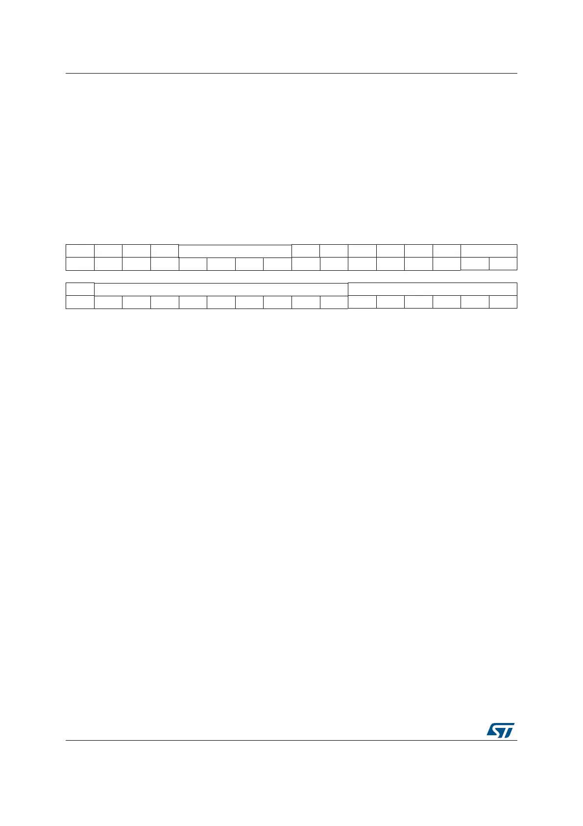
6.3.24 RCC PLL configuration register (RCC_PLLSAICFGR)
Address offset: 0x88
Reset value: 0x2400 3000
Access: no wait state, word, half-word and byte access.
This register is used to configure the PLLSAI clock outputs according to the formulas:
• f
(VCO clock)
= f
(PLLSAI clock input)
× (PLLSAIN / PLLM)
• f
(PLL SAI 48MHz clock output)
= f
(VCO clock)
/ PLLSAIP
• f
(PLL SAI1 clock output)
= f
(VCO clock)
/ PLLSAIQ
31 30 29 28 27 26 25 24 23 22 21 20 19 18 17 16
Res. Res. Res. Res. PLLSAIQ[3:0] Res. Res. Res. Res. Res. Res. PLLSAIP[1:0]
rw rw rw rw rw rw
1514131211109876543210
Res. PLLSAIN[8:0] PLLSAIM[5:0]
rw rw rw rw rw rw rw rw rw rw rw rw rw rw rw
Bits 31:28 Reserved, must be kept at reset value.
Bits 27:24 PLLSAIQ: PLLSAI division factor for SAIs clock
Set and reset by software to control the frequency of SAIs clock.
These bits should be written when the PLLSAI is disabled.
SAI1 clock frequency = VCO frequency / PLLSAIQ with 2 PLLSAIQ 15
0000: PLLSAIQ = 0, wrong configuration
0001: PLLSAIQ = 1, wrong configuration
...
0010: PLLSAIQ = 2
0011: PLLSAIQ = 3
0100: PLLSAIQ = 4
0101: PLLSAIQ = 5
...
1111: PLLSAIQ = 15
Bits 23:18 Reserved, must be kept at reset value.
Bits 17:16 PLLSAIP: PLLSAI division factor for 48 MHz clock
These bits are set and cleared by software to control the output clock frequency.
They should be written when the PLLSAI is disabled.
Caution: The software has to set these bits correctly to ensure that the output frequency not
exceed 120 MHz on this output
PLL output clock frequency = VCO frequency / PLLSAIP with PLLSAIP = 2, 4, 6 or 8
00: PLLSAIP =2
01: PLLSAIP = 4
10: PLLSAIP = 6
11: PLLSAIP = 8