RM0390 Rev 4 1021/1328
RM0390 Secure digital input/output interface (SDIO)
1031
29.8.8 SDIO data length register (SDIO_DLEN)
Address offset: 0x28
Reset value: 0x0000 0000
The SDIO_DLEN register contains the number of data bytes to be transferred. The value is
loaded into the data counter when data transfer starts.
Note: For a block data transfer, the value in the data length register must be a multiple of the block
size (see SDIO_DCTRL). A data transfer must be written to the data timer register and the
data length register before being written to the data control register.
For an SDIO multibyte transfer the value in the data length register must be between 1 and
512.
29.8.9 SDIO data control register (SDIO_DCTRL)
Address offset: 0x2C
Reset value: 0x0000 0000
The SDIO_DCTRL register control the data path state machine (DPSM).
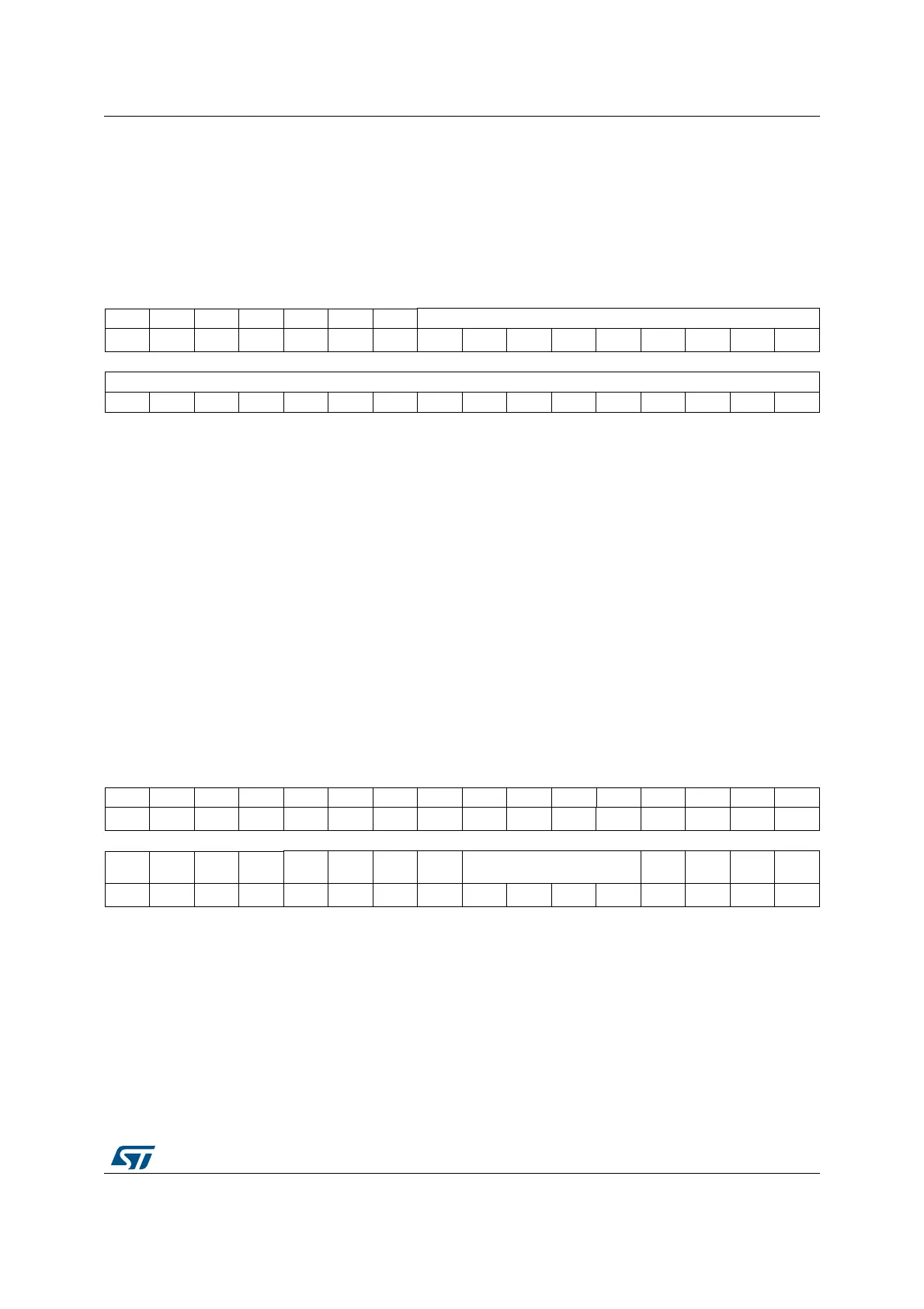
31 30 29 28 27 26 25 24 23 22 21 20 19 18 17 16
Res. Res. Res. Res. Res. Res. Res. DATALENGTH[24:16]
rw rw rw rw rw rw rw rw rw
1514131211109876543210
DATALENGTH[15:0]
rw rw rw rw rw rw rw rw rw rw rw rw rw rw rw rw
Bits 31:25 Reserved, must be kept at reset value.
Bits 24:0 DATALENGTH: Data length value
Number of data bytes to be transferred.
31 30 29 28 27 26 25 24 23 22 21 20 19 18 17 16
Res. Res. Res. Res. Res. Res. Res. Res. Res. Res. Res. Res. Res. Res. Res. Res.
1514131211109876543210
Res. Res. Res. Res.
SDIO
EN
RW
MOD
RW
STOP
RW
START
DBLOCKSIZE
DMA
EN
DT
MODE
DTDIR DTEN
rw rw rw rw rw rw rw rw rw rw rw rw
Bits 31:12 Reserved, must be kept at reset value.
Bit 11 SDIOEN: SD I/O enable functions
If this bit is set, the DPSM performs an SD I/O-card-specific operation.
Bit 10 RWMOD: Read wait mode
0: Read Wait control stopping SDIO_D2
1: Read Wait control using SDIO_CK
 Loading...


