Analog-to-digital converter (ADC) RM0390
388/1328 RM0390 Rev 4
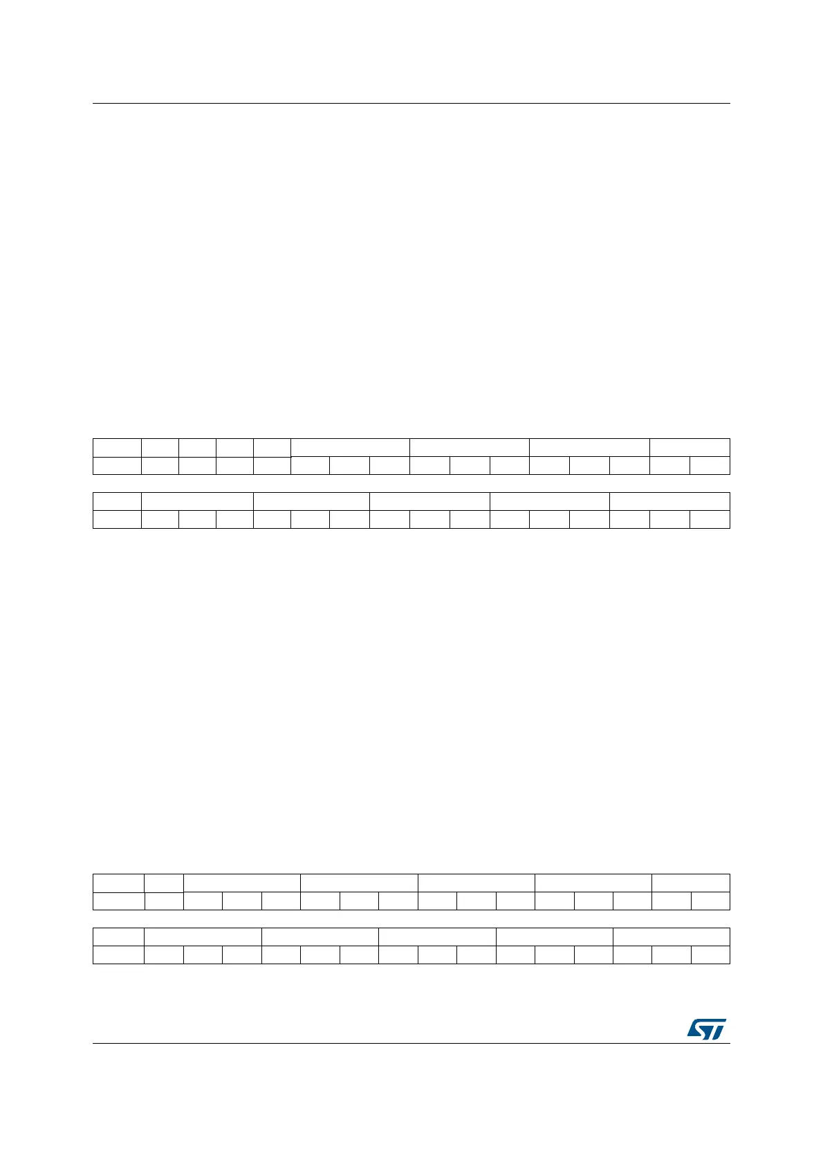
13.13.4 ADC sample time register 1 (ADC_SMPR1)
Address offset: 0x0C
Reset value: 0x0000 0000
13.13.5 ADC sample time register 2 (ADC_SMPR2)
Address offset: 0x10
Reset value: 0x0000 0000
Bits 7:2 Reserved, must be kept at reset value.
Bit 1 CONT: Continuous conversion
This bit is set and cleared by software. If it is set, conversion takes place continuously until it
is cleared.
0: Single conversion mode
1: Continuous conversion mode
Bit 0 ADON: A/D Converter ON / OFF
This bit is set and cleared by software.
Note: 0: Disable ADC conversion and go to power down mode
1: Enable ADC
31 30 29 28 27 26 25 24 23 22 21 20 19 18 17 16
Res. Res. Res. Res. Res. SMP18[2:0] SMP17[2:0] SMP16[2:0] SMP15[2:1]
rw rw rw rw rw rw rw rw rw rw rw
15 14 13 12 11 10 9 8 7 6 5 4 3 2 1 0
SMP15_0 SMP14[2:0] SMP13[2:0] SMP12[2:0] SMP11[2:0] SMP10[2:0]
rw rw rw rw rw rw rw rw rw rw rw rw rw rw rw rw
Bits 31: 27 Reserved, must be kept at reset value.
Bits 26:0 SMPx[2:0]: Channel x sampling time selection
These bits are written by software to select the sampling time individually for each channel.
During sampling cycles, the channel selection bits must remain unchanged.
Note: 000: 3 cycles
001: 15 cycles
010: 28 cycles
011: 56 cycles
100: 84 cycles
101: 112 cycles
110: 144 cycles
111: 480 cycles
31 30 29 28 27 26 25 24 23 22 21 20 19 18 17 16
Res. Res. SMP9[2:0] SMP8[2:0] SMP7[2:0] SMP6[2:0] SMP5[2:1]
rw rw rw rw rw rw rw rw rw rw rw rw rw rw
1514131211109876543210
SMP5_0 SMP4[2:0] SMP3[2:0] SMP2[2:0] SMP1[2:0] SMP0[2:0]
rw rw rw rw rw rw rw rw rw rw rw rw rw rw rw rw