Debug support (DBG) RM0390
1312/1328 RM0390 Rev 4
This register is mapped on the external PPB and is reset by the PORESET (and not by the
SYSTEM reset). It can be written by the debugger under SYSTEM reset.
Note: By default, the TRACECLKIN input clock of the TPIU is tied to GND. It is assigned to HCLK
two clock cycles after the bit TRACE_IOEN has been set.
The debugger must then program the Trace Mode by writing the PROTOCOL[1:0] bits in the
SPP_R (Selected Pin Protocol) register of the TPIU.
• PROTOCOL=00: Trace Port Mode (synchronous)
• PROTOCOL=01 or 10: Serial Wire (Manchester or NRZ) Mode (asynchronous mode).
Default state is 01
It then also configures the TRACE port size by writing the bits [3:0] in the CPSPS_R
(Current Sync Port Size Register) of the TPIU:
• 0x1 for 1 pin (default state)
• 0x2 for 2 pins
• 0x8 for 4 pins
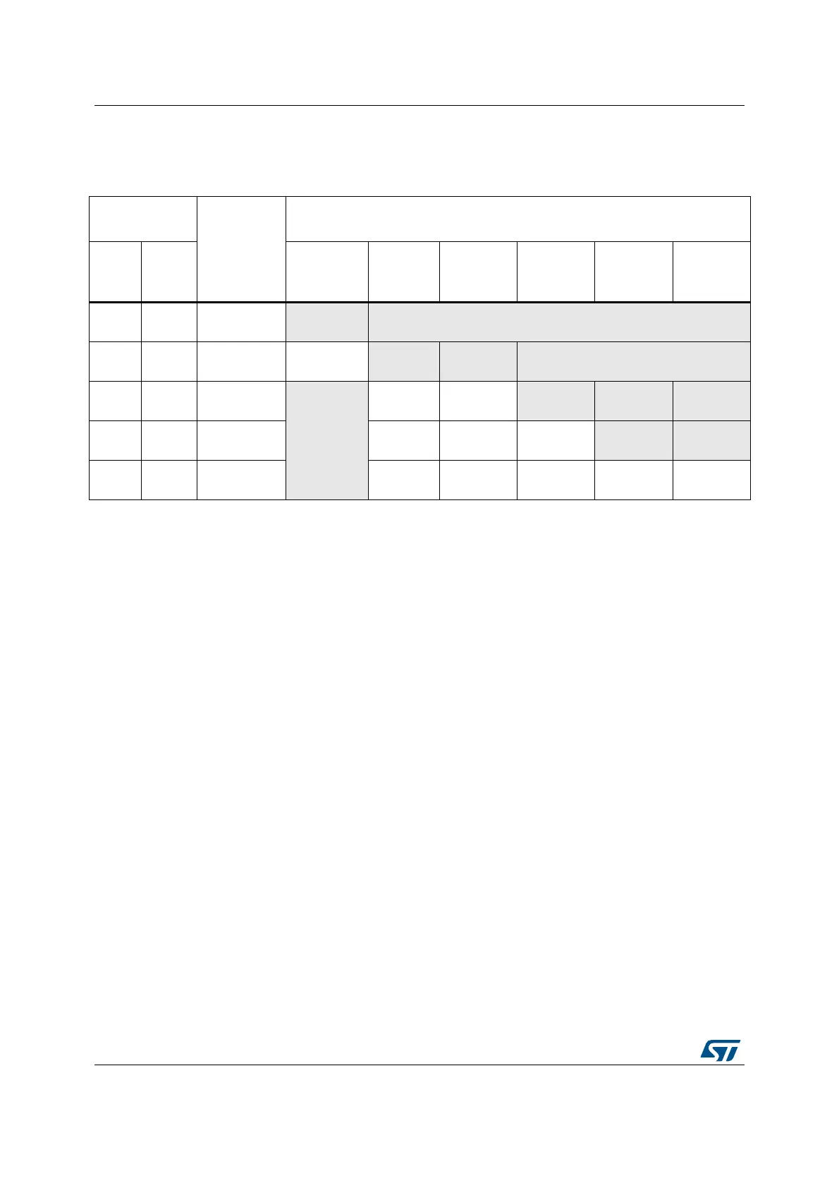
Table 251. Flexible TRACE pin assignment
DBGMCU_CR
register
Pins
assigned
for:
TRACE IO pin assigned
TRACE
_IOEN
TRACE
_MODE
[1:0]
PB3 /JTDO/
TRACESWO
PE2/
TRACECK
TRACED[0]
(1)
TRACED[1]
(1)
TRACED[2]
(1)
TRACED[3]
(1)
0XX
No Trace
(default state)
Released
(2)
-
100
Asynchronous
Trace
TRACESWO
- -
Released
(usable as GPIO)
101
Synchronous
Trace 1 bit
Released
(2)
TRACECK TRACED[0] - - -
110
Synchronous
Trace 2 bit
TRACECK TRACED[0] TRACED[1]
- -
111
Synchronous
Trace 4 bit
TRACECK TRACED[0] TRACED[1] TRACED[2] TRACED[3]
1. Refer to the Alternate function mapping table in the datasheets.
2. When Serial Wire mode is used, it is released. But when JTAG is used, it is assigned to JTDO.
 Loading...


