Secure digital input/output interface (SDIO) RM0390
978/1328 RM0390 Rev 4
29.3.1 SDIO adapter
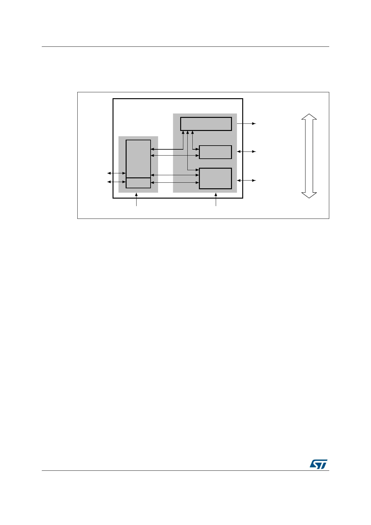
Figure 376 shows a simplified block diagram of an SDIO adapter.
Figure 376. SDIO adapter
The SDIO adapter is a multimedia/secure digital memory card bus master that provides an
interface to a multimedia card stack or to a secure digital memory card. It consists of five
subunits:
• Adapter register block
• Control unit
• Command path
• Data path
• Data FIFO
Note: The adapter registers and FIFO use the APB2 bus clock domain (PCLK2). The control unit,
command path and data path use the SDIO adapter clock domain (SDIOCLK).
Adapter register block
The adapter register block contains all system registers. This block also generates the
signals that clear the static flags in the multimedia card. The clear signals are generated
when 1 is written into the corresponding bit location in the SDIO Clear register.
Control unit
The control unit contains the power management functions and the clock divider for the
memory card clock.
There are three power phases:
• power-off
• power-up
• power-on
06Y9
7R$3%
LQWHUIDFH
&RQWUROXQLW
&RPPDQG
SDWK
'DWDSDWK
$GDSWHU
UHJLVWHUV
6',2B&.
6',2B&0'
6',2B'>@
6',2DGDSWHU
3&/. 6',2&/.
),)2
&DUGEXV