Analog-to-digital converter (ADC) RM0390
394/1328 RM0390 Rev 4
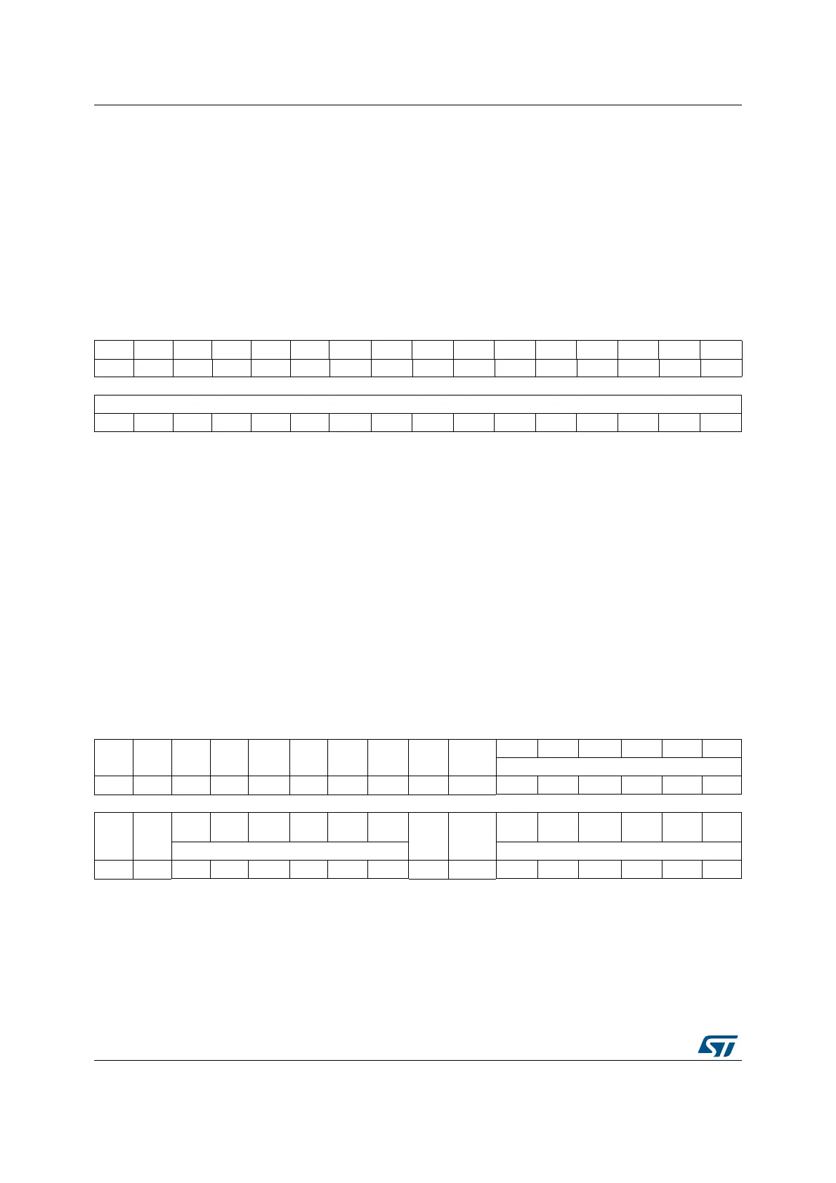
13.13.14 ADC regular data register (ADC_DR)
Address offset: 0x4C
Reset value: 0x0000 0000
13.13.15 ADC Common status register (ADC_CSR)
Address offset: 0x00 (this offset address is relative to ADC1 base address + 0x300)
Reset value: 0x0000 0000
This register provides an image of the status bits of the different ADCs. Nevertheless it is
read-only and does not allow to clear the different status bits. Instead each status bit must
be cleared by writing it to 0 in the corresponding ADC_SR register.
Bits 31:16 Reserved, must be kept at reset value.
Bits 15:0 JDATA[15:0]: Injected data
These bits are read-only. They contain the conversion result from injected channel x. The
data are left -or right-aligned as shown in Figure 76 and Figure 77.
31 30 29 28 27 26 25 24 23 22 21 20 19 18 17 16
Res. Res. Res. Res. Res. Res. Res. Res. Res. Res. Res. Res. Res. Res. Res. Res.
15 14 13 12 11 10 9 8 7 6 5 4 3 2 1 0
DATA[15:0]
rrrrrrrrrrrrrrrr
Bits 31:16 Reserved, must be kept at reset value.
Bits 15:0 DATA[15:0]: Regular data
These bits are read-only. They contain the conversion result from the regular
channels. The data are left- or right-aligned as shown in Figure 76 and
Figure 77.
31 30 29 28 27 26 25 24 23 22 21 20 19 18 17 16
Res. Res. Res. Res. Res. Res. Res. Res. Res. Res.
OVR3 STRT3 JSTRT3 JEOC 3 EOC3 AWD3
ADC3
rrrrrr
15 14 13 12 11 10 9 8 7 6 5 4 3 2 1 0
Res. Res.
OVR2 STRT2
JSTRT
2
JEOC2 EOC2 AWD2
Res. Res.
OVR1 STRT1 JSTRT1 JEOC 1 EOC1 AWD1
ADC2 ADC1
rr rrr r r r r r r r
Bits 31:22 Reserved, must be kept at reset value.
Bit 21 OVR3: Overrun flag of ADC3
This bit is a copy of the OVR bit in the ADC3_SR register.
Bit 20 STRT3: Regular channel Start flag of ADC3
This bit is a copy of the STRT bit in the ADC3_SR register.
 Loading...


