RM0390 Rev 4 405/1328
RM0390 Digital-to-analog converter (DAC)
422
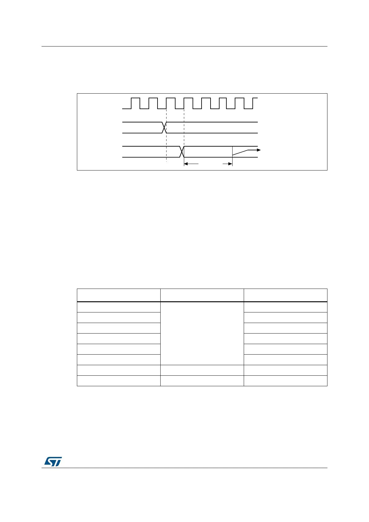
When DAC_DORx is loaded with the DAC_DHRx contents, the analog output voltage
becomes available after a time t
SETTLING
that depends on the power supply voltage and the
analog output load.
Figure 96. Timing diagram for conversion with trigger disabled TEN = 0
14.3.5 DAC output voltage
Digital inputs are converted to output voltages on a linear conversion between 0 and V
REF+
.
The analog output voltages on each DAC channel pin are determined by the following
equation:
14.3.6 DAC trigger selection
If the TENx control bit is set, conversion can then be triggered by an external event (timer
counter, external interrupt line). The TSELx[2:0] control bits determine which out of 8
possible events will trigger conversion as shown in Table 94.
Each time a DAC interface detects a rising edge on the selected timer TRGO output, or on
the selected external interrupt line 9, the last data stored into the DAC_DHRx register are
transferred into the DAC_DORx register. The DAC_DORx register is updated three APB1
cycles after the trigger occurs.
!0"?#,+
X!#
X!#
T
3%44,).'
$(2
$/2
/UTPUTVOLTAGE
AVAILABLEON$!#?/54PIN
AIB
DACoutput V
REF
DOR
4096
--------------
×=
Table 94. External triggers
Source Type TSEL[2:0]
Timer 6 TRGO event
Internal signal from on-chip
timers
000
Timer 8 TRGO event 001
Timer 7 TRGO event 010
Timer 5 TRGO event 011
Timer 2 TRGO event 100
Timer 4 TRGO event 101
EXTI line9 External pin 110
SWTRIG Software control bit 111