RM0390 Rev 4 259/1328
RM0390 Flexible memory controller (FMC)
324
The FMC supports a wide range of devices through a programmable timings among which:
• Programmable wait states (up to 15)
• Programmable bus turnaround cycles (up to 15)
• Programmable output enable and write enable delays (up to 15)
• Independent read and write timings and protocol to support the widest variety of
memories and timings
• Programmable continuous clock (FMC_CLK) output.
The FMC Clock (FMC_CLK) is a submultiple of the HCLK clock. It can be delivered to the
selected external device either during synchronous accesses only or during asynchronous
and synchronous accesses depending on the CCKEN bit configuration in the FMC_BCR1
register:
• If the CCLKEN bit is reset, the FMC generates the clock (CLK) only during
synchronous accesses (Read/write transactions).
• If the CCLKEN bit is set, the FMC generates a continuous clock during asynchronous
and synchronous accesses. To generate the FMC_CLK continuous clock, Bank 1 must
be configured in synchronous mode (see Section 11.5.6: NOR/PSRAM controller
registers). Since the same clock is used for all synchronous memories, when a
continuous output clock is generated and synchronous accesses are performed, the
AHB data size has to be the same as the memory data width (MWID) otherwise the
FMC_CLK frequency will be changed depending on AHB data transaction (refer to
Section 11.5.5: Synchronous transactions for FMC_CLK divider ratio formula).
The size of each bank is fixed and equal to 64 Mbytes. Each bank is configured through
dedicated registers (see Section 11.5.6: NOR/PSRAM controller registers).
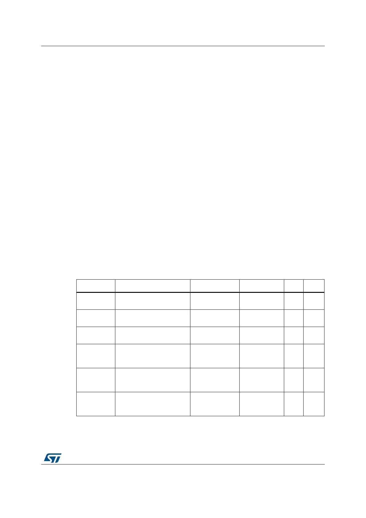
The programmable memory parameters include access times (see Table 48) and support
for wait management (for PSRAM and NOR Flash accessed in burst mode).
Table 48. Programmable NOR/PSRAM access parameters
Parameter Function Access mode Unit Min. Max.
Address
setup
Duration of the address
setup phase
Asynchronous
AHB clock cycle
(HCLK)
015
Address hold
Duration of the address hold
phase
Asynchronous,
muxed I/Os
AHB clock cycle
(HCLK)
115
Data setup
Duration of the data setup
phase
Asynchronous
AHB clock cycle
(HCLK)
1256
Bust turn
Duration of the bus
turnaround phase
Asynchronous and
synchronous read
/ write
AHB clock cycle
(HCLK)
015
Clock divide
ratio
Number of AHB clock cycles
(HCLK) to build one memory
clock cycle (CLK)
Synchronous
AHB clock cycle
(HCLK)
2 16
Data latency
Number of clock cycles to
issue to the memory before
the first data of the burst
Synchronous
Memory clock
cycle (CLK)
2 17