RM0390 Rev 4 179/1328
RM0390 General-purpose I/Os (GPIO)
194
In addition to this flexible I/O multiplexing architecture, each peripheral has alternate
functions mapped onto different I/O pins to optimize the number of peripherals available in
smaller packages.
To use an I/O in a given configuration, proceed as follows:
• System function
Connect the I/O to AF0 and configure it depending on the function used:
– JTAG/SWD, after each device reset these pins are assigned as dedicated pins
immediately usable by the debugger host (not controlled by the GPIO controller)
– RTC_REFIN: this pin should be configured in Input floating mode
– MCO1 and MCO2: these pins have to be configured in alternate function mode.
Note: You can disable some or all of the JTAG/SWD pins and so release the associated pins for
GPIO usage.
For more details refer to Section 6.2.10: Clock-out capability.
• GPIO
Configure the desired I/O as output or input in the GPIOx_MODER register.
• Peripheral alternate function
For the ADC and DAC, configure the desired I/O as analog in the GPIOx_MODER
register.
For other peripherals:
– Configure the desired I/O as an alternate function in the GPIOx_MODER register
– Select the type, pull-up/pull-down and output speed via the GPIOx_OTYPER,
GPIOx_PUPDR and GPIOx_OSPEEDER registers, respectively
– Connect the I/O to the desired AFx in the GPIOx_AFRL or GPIOx_AFRH register
• EVENTOUT
Configure the I/O pin used to output the Cortex
®
-M4 with FPU EVENTOUT signal by
connecting it to AF15
Note: EVENTOUT is not mapped onto the following I/O pins: PC13, PC14, PC15, PH0 and PH1.
Refer to the “Alternate function mapping” table in the datasheets for the detailed mapping of
the system and peripherals’ alternate function I/O pins.
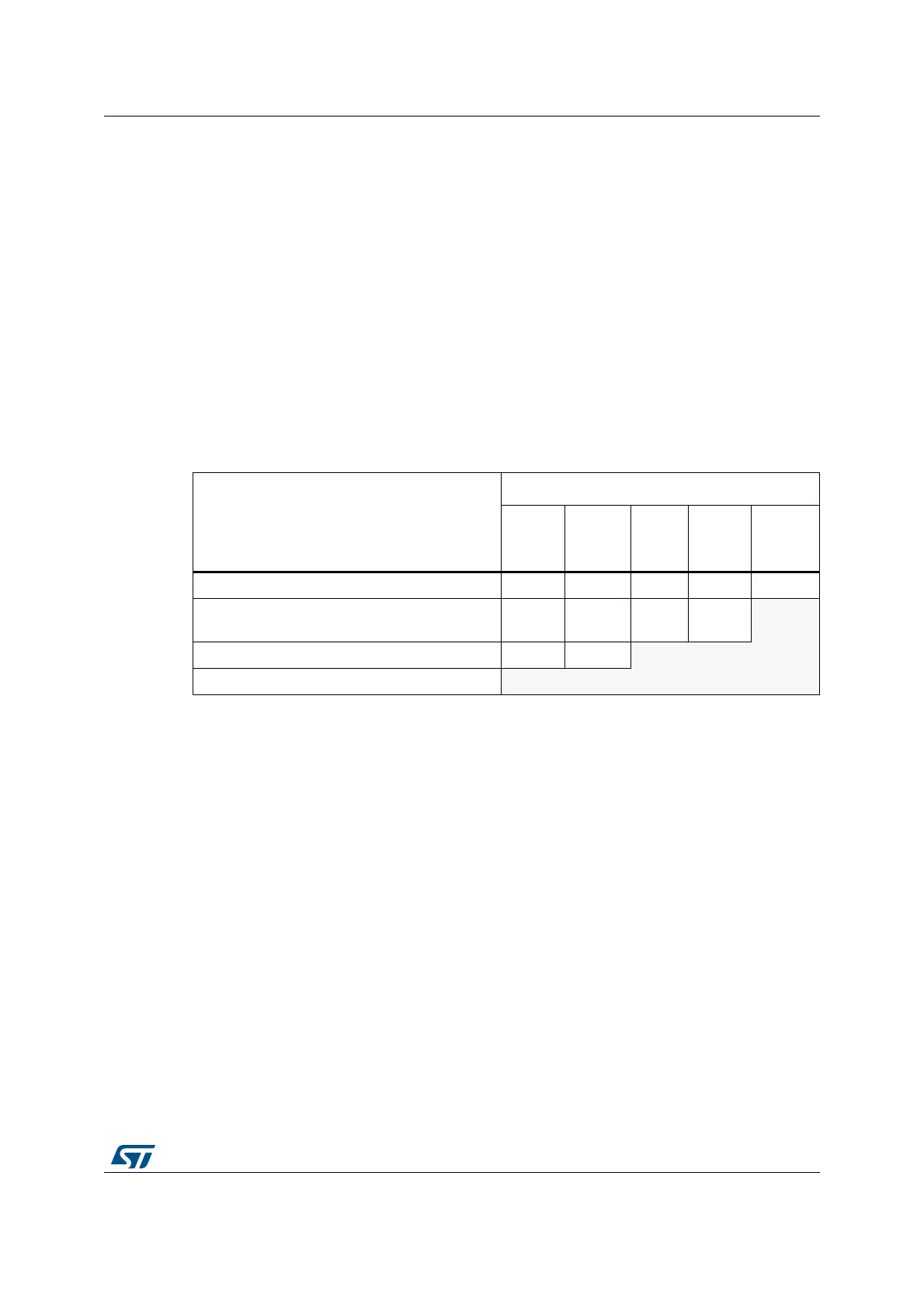
Table 23. Flexible SWJ-DP pin assignment
Available debug ports
SWJ I/O pin assigned
PA13 /
JTMS/
SWDIO
PA14 /
JTCK/
SWCLK
PA15 /
JTDI
PB3 /
JTDO
PB4/
NJTRST
Full SWJ (JTAG-DP + SW-DP) - Reset state X X X X X
Full SWJ (JTAG-DP + SW-DP) but without
NJTRST
XXXX
JTAG-DP Disabled and SW-DP Enabled X X
JTAG-DP Disabled and SW-DP Disabled Released
 Loading...


