RM0390 Rev 4 1083/1328
RM0390 USB on-the-go full-speed/high-speed (OTG_FS/OTG_HS)
1264
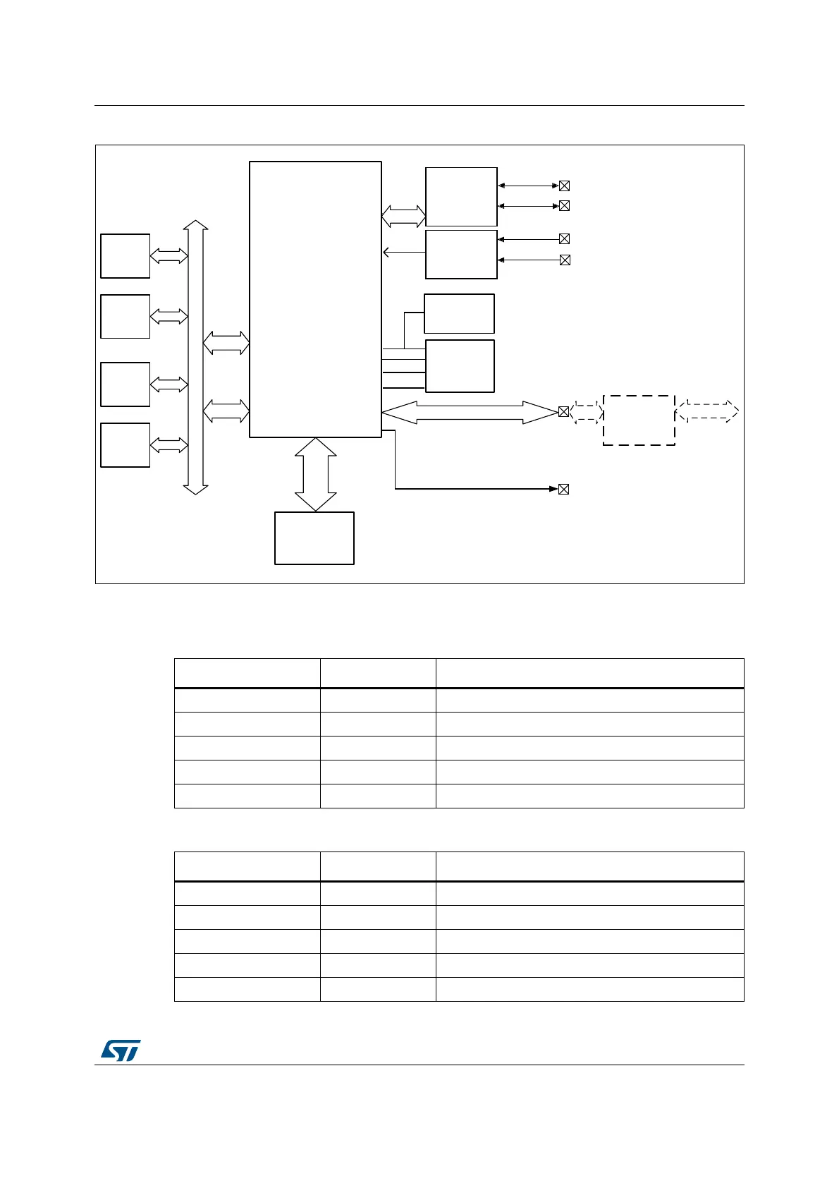
Figure 401. OTG high-speed block diagram
31.4.2 USB OTG pin and internal signals
06Y9
'DWD),)2
6LQJOHSRUW5$0
635$0
$+%
PDVWHU
LQWHUIDFH
$+%
VODYH
LQWHUIDFH
&38
0HPRU\
3HULSKHUDO
3HULSKHUDO
'DWD),)2
5$0LQWHUIDFH
$+%DSSOLFDWLRQEXV
27*B+6
86%27*+6FRUH
27*B+6B'3
27*B+6B'0
27*B+6B,'
27*B+6B9%86
27*)63+<
WUDQVFHLYHU
27*B+6B62)
8/3,LQWHUIDFHSLQV
8/3,3+<
H[WHUQDO
FRPSRQHQW
86%''
8/3,B&.
8/3,B',5
8/3,B673
8/3,B1;7
8/3,B'
19,&
,QWHUUXSW(3RXW
,QWHUUXSW(3LQ
,QWHUUXSWJOREDO
,QWHUUXSWDV\QFZDNHXS
27*GHWHFWLRQV
(;7,(;7,
VHULDO
Table 219. OTG_FS input/output pins
Signal name Signal type Description
OTG_FS_DP Digital input/output USB OTG D+ line
OTG_FS_DM Digital input/output USB OTG D- line
OTG_FS_ID Digital input USB OTG ID
OTG_FS_VBUS Analog input USB OTG VBUS
OTG_FS_SOF Digital output USB OTG Start Of Frame (visibility)
Table 220. OTG_HS input/output pins
Signal name Signal type Description
OTG_HS_DP Digital input/output USB OTG D+ line
OTG_HS_DM Digital input/output USB OTG D- line
OTG_HS_ID Digital input USB OTG ID
OTG_HS_VBUS Analog input USB OTG VBUS
OTG_HS_SOF Digital output USB OTG Start Of Frame (visibility)
 Loading...


