RM0390 Rev 4 129/1328
RM0390 Reset and clock control (RCC)
175
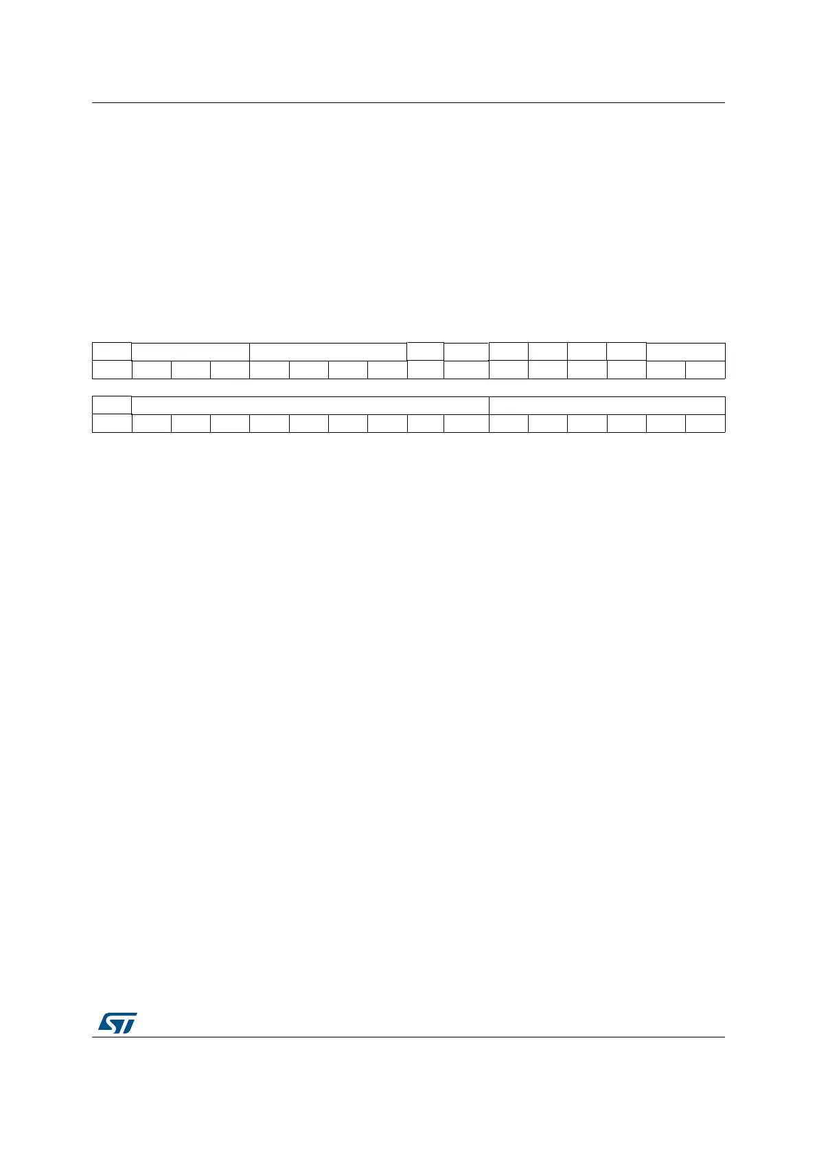
6.3.2 RCC PLL configuration register (RCC_PLLCFGR)
Address offset: 0x04
Reset value: 0x2400 3010
Access: no wait state, word, half-word and byte access.
This register is used to configure the PLL clock outputs according to the formulas:
• f
(VCO clock)
= f
(PLL clock input)
× (PLLN / PLLM)
• f
(PLL general clock output)
= f
(VCO clock)
/ PLLP
• f
(USB OTG FS, SDIO)
= f
(VCO clock)
/ PLLQ
31 30 29 28 27 26 25 24 23 22 21 20 19 18 17 16
Res. PLLR[2:0] PLLQ[3:0] Res. PLLSRC Res. Res. Res. Res. PLLP[1:0]
rw rw rw rw rw rw rw rw rw rw
15 14 13 12 11 10 9 8 7 6 5 4 3 2 1 0
Res. PLLN[8:0] PLLM[5:0]
rw rw rw rw rw rw rw rw rw rw rw rw rw rw rw
Bit 31 Reserved, must be kept at reset value.
Bits 30:28 PLLR[2:0]: Main PLL division factor for I2Ss, SAIs, SYSTEM and SPDIF-Rx clocks
Set and cleared by software to control the frequency of the clock. These bits should be
written only if PLL is disabled.
Clock frequency = VCO frequency / PLLR with 2 PLLR 7
000: PLLR = 0, wrong configuration
001: PLLR = 1, wrong configuration
010: PLLR = 2
011: PLLR = 3
...
111: PLLR = 7
Bits 27:24 PLLQ[3:0]: Main PLL (PLL) division factor for USB OTG FS, SDIOclocks
Set and cleared by software to control the frequency of USB OTG FS clock and the
SDIOclock. These bits should be written only if PLL is disabled.
Caution: The USB OTG FS requires a 48 MHz clock to work correctly. The SDIOneeds a
frequency lower than or equal to 48 MHz to work correctly.
USB OTG FS clock frequency = VCO frequency / PLLQ with 2
PLLQ 15
0000: PLLQ = 0, wrong configuration
0001: PLLQ = 1, wrong configuration
0010: PLLQ = 2
0011: PLLQ = 3
0100: PLLQ = 4
...
1111: PLLQ = 15
Bit 23 Reserved, must be kept at reset value.
Bit 22 PLLSRC: Main PLL(PLL) and audio PLL (PLLI2S) entry clock source
Set and cleared by software to select PLL and PLLI2S clock source. This bit can be written
only when PLL and PLLI2S are disabled.
0: HSI clock selected as PLL and PLLI2S clock entry
1: HSE oscillator clock selected as PLL and PLLI2S clock entry