RM0390 Rev 4 1167/1328
RM0390 USB on-the-go full-speed/high-speed (OTG_FS/OTG_HS)
1264
31.15.39 OTG device V
BUS
discharge time register
(OTG_DVBUSDIS)
Address offset: 0x0828
Reset value: 0x0000 17D7
This register specifies the V
BUS
discharge time after V
BUS
pulsing during SRP.
31.15.40 OTG device V
BUS
pulsing time register
(OTG_DVBUSPULSE)
Address offset: 0x082C
Reset value: 0x0000 05B8
This register specifies the V
BUS
pulsing time during SRP.
Bits 31:16 OEPM[15:0]: OUT EP interrupt mask bits
One per OUT endpoint:
Bit 16 for OUT EP 0, bit 19 for OUT EP 3
0: Masked interrupt
1: Unmasked interrupt
Bits 15:0 IEPM[15:0]: IN EP interrupt mask bits
One bit per IN endpoint:
Bit 0 for IN EP 0, bit 3 for IN EP 3
0: Masked interrupt
1: Unmasked interrupt
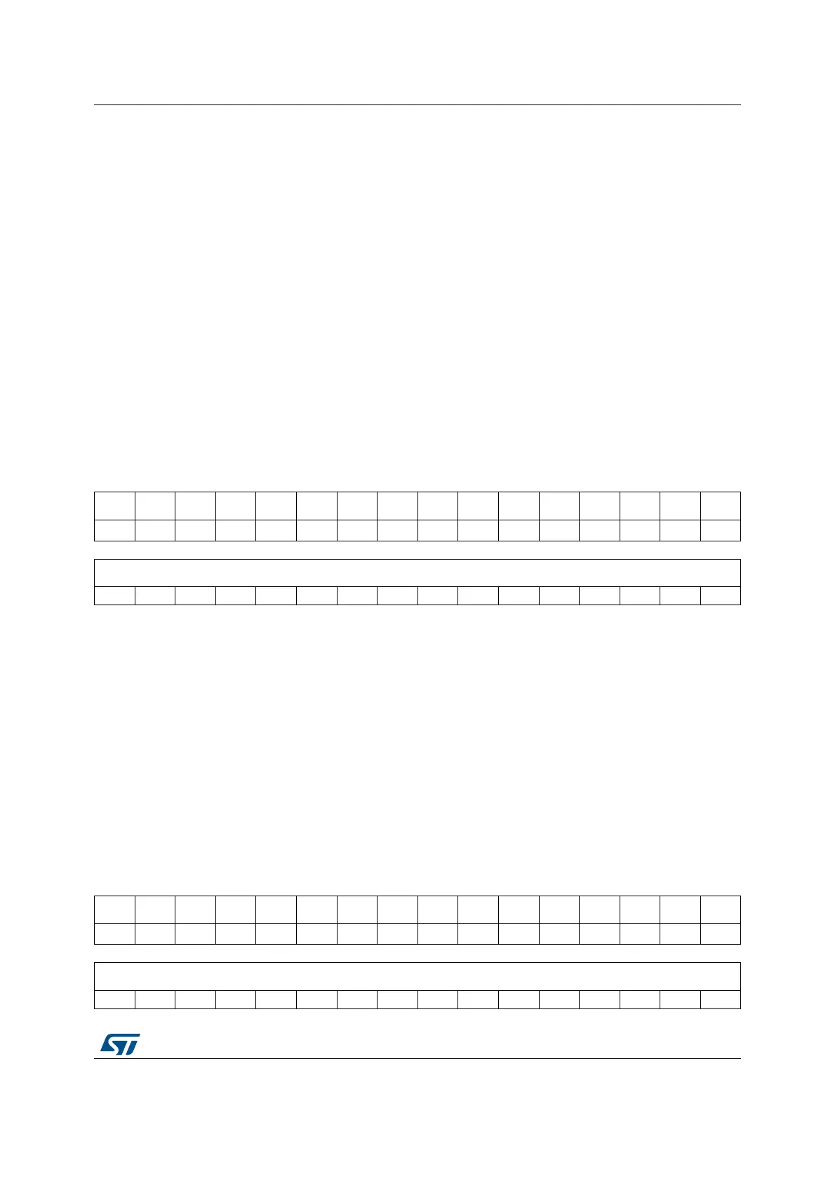
31 30 29 28 27 26 25 24 23 22 21 20 19 18 17 16
Res. Res. Res. Res. Res. Res. Res. Res. Res. Res. Res. Res. Res. Res. Res. Res.
1514131211109876543210
VBUSDT[15:0]
rw rw rw rw rw rw rw rw rw rw rw rw rw rw rw rw
Bits 31:16 Reserved, must be kept at reset value.
Bits 15:0 VBUSDT[15:0]: Device V
BUS
discharge time
Specifies the V
BUS
discharge time after V
BUS
pulsing during SRP. This value equals:
V
BUS
discharge time in PHY clocks / 1 024
Depending on your V
BUS
load, this value may need adjusting.
31 30 29 28 27 26 25 24 23 22 21 20 19 18 17 16
Res. Res. Res. Res. Res. Res. Res. Res. Res. Res. Res. Res. Res. Res. Res. Res.
1514131211109876543210
DVBUSP[15:0]
rw rw rw rw rw rw rw rw rw rw rw rw rw rw rw rw
 Loading...


