RM0390 Rev 4 169/1328
RM0390 Reset and clock control (RCC)
175
6.3.26 RCC clocks gated enable register (CKGATENR)
Address offset: 0x90
Reset value: 0x0000 0000
Access: no wait state, word, half-word and byte access.
This register allows to enable or disable the clock gating for the specified IPs.
Bits 12:8 PLLSAIDIVQ[4:0]: PLLSAI division factor for SAIs clock
These bits are set and reset by software to control the SAIs clock frequency.
They should be written only if PLLSAI is disabled.
SAI1 clock frequency = f(PLLSAI_Q) / PLLSAIDIVQ with 1
PLLSAIDIVQ 31
00000: PLLSAIDIVQ = /1
00001: PLLSAIDIVQ = /2
00010: PLLSAIDIVQ = /3
00011: PLLSAIDIVQ = /4
00100: PLLSAIDIVQ = /5
...
11111: PLLSAIDIVQ = /32
Bits 7:5 Reserved, must be kept at reset value.
Bits 4:0 PLLI2SDIVQ[4:0]: PLLI2S division factor for SAIs clock
These bits are set and reset by software to control the SAIs clock frequency.
They should be written only if PLLI2S is disabled.
SAI1 clock frequency = f(PLLI2S_Q) / PLLI2SDIVQ with 1 PLLI2SDIVQ 31
00000: PLLI2SDIVQ = /1
00001: PLLI2SDIVQ = /2
00010: PLLI2SDIVQ = /3
00011: PLLI2SDIVQ = /4
00100: PLLI2SDIVQ = /5
...
11111: PLLI2SDIVQ = /32
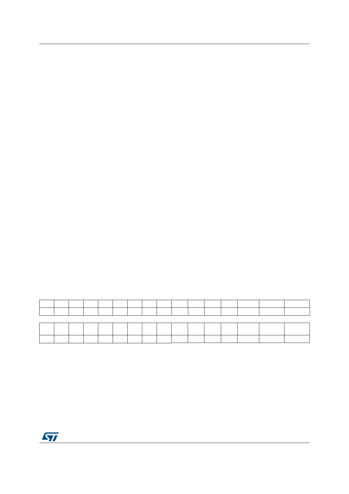
31 30 29 28 27 26 25 24 23 22 21 20 19 18 17 16
Res. Res. Res. Res. Res. Res. Res. Res. Res. Res. Res. Res. Res. Res. Res. Res.
15 14 13 12 11 10 9 8 7 6 5 4 3 2 1 0
Res. Res. Res. Res. Res. Res. Res. Res. Res.
RCC
_CKEN
FLITF
_CKEN
SRAM
_CKEN
SPARE
_CKEN
CM4DBG
_CKEN
AHB2APB2
_CKEN
AHB2APB1
_CKEN
rw rw rw rw rw rw rw
Bits 31:7 Reserved, must be kept at reset value.
Bit 6
RCC_CKEN: RCC clock enable
0: the clock gating is enabled
1: the clock gating is disabled, the clock is always enabled.
Bit 5
FLITF_CKEN: Flash Interface clock enable
0: the clock gating is enabled
1: the clock gating is disabled, the clock is always enabled.
 Loading...


