RM0390 Rev 4 265/1328
RM0390 Flexible memory controller (FMC)
324
The one HCLK cycle at the end of the write transaction helps guarantee the address and
data hold time after the NWE rising edge. Due to the presence of this HCLK cycle, the
DATAST value must be greater than zero (DATAST > 0).
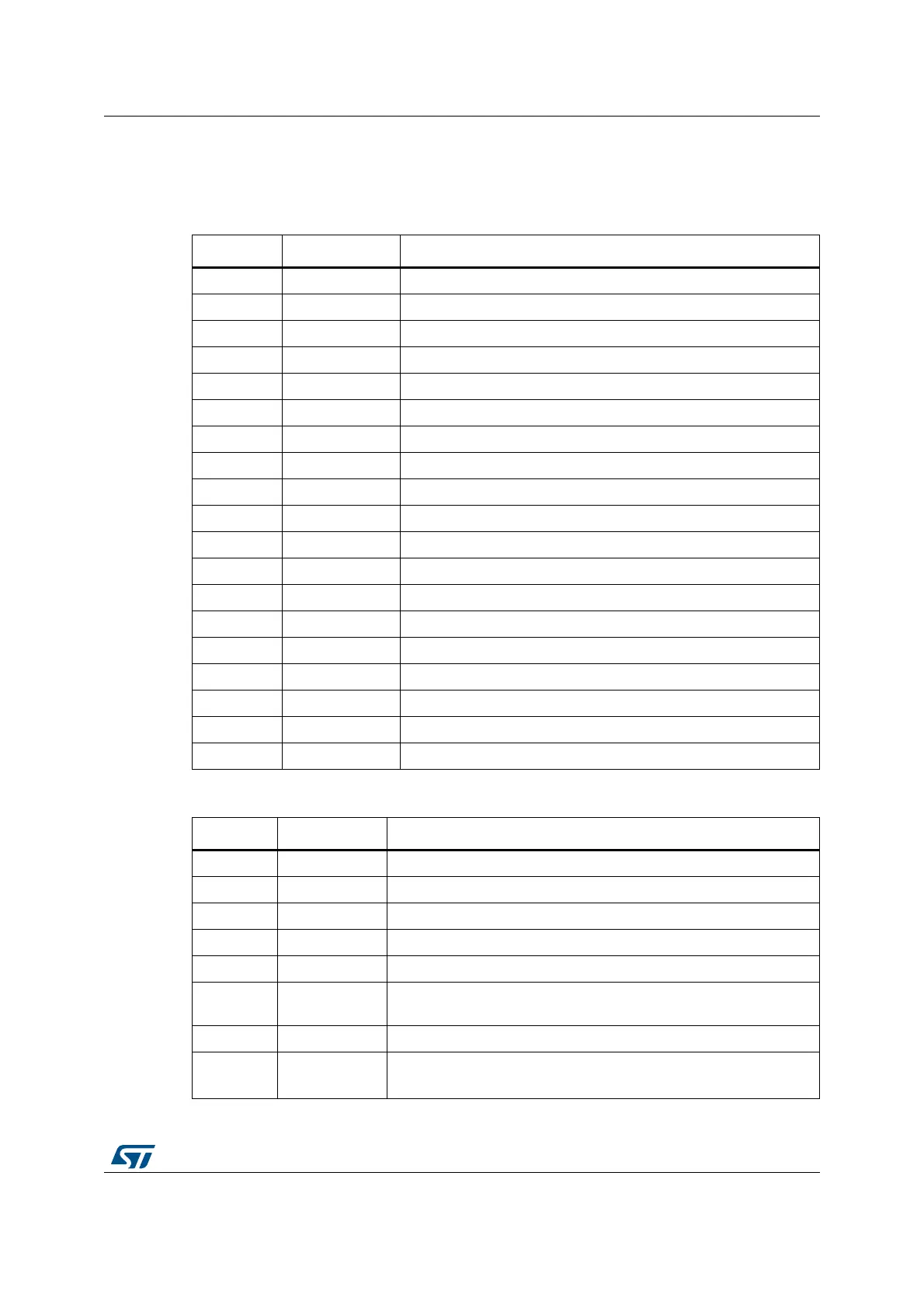
Table 54. FMC_BCRx bit fields
Bit number Bit name Value to set
31:22 Reserved 0x000
21 WFDIS As needed
20 CCLKEN As needed
19 CBURSTRW 0x0 (no effect in asynchronous mode)
18:16 CPSIZE 0x0 (no effect in asynchronous mode)
15 ASYNCWAIT Set to 1 if the memory supports this feature. Otherwise keep at 0.
14 EXTMOD 0x0
13 WAITEN 0x0 (no effect in asynchronous mode)
12 WREN As needed
11 Reserved 0x0
10 Reserved 0x0
9 WAITPOL Meaningful only if bit 15 is 1
8 BURSTEN 0x0
7 Reserved 0x1
6 FACCEN Don’t care
5:4 MWID As needed
3:2 MTYP As needed, exclude 0x2 (NOR Flash memory)
1 MUXE 0x0
0 MBKEN 0x1
Table 55. FMC_BTRx bit fields
Bit number Bit name Value to set
31:30 Reserved 0x0
29:28 ACCMOD Don’t care
27:24 DATLAT Don’t care
23:20 CLKDIV Don’t care
19:16 BUSTURN Time between NEx high to NEx low (BUSTURN HCLK).
15:8 DATAST
Duration of the second access phase (DATAST+1 HCLK cycles for
write accesses, DATAST HCLK cycles for read accesses).
7:4 ADDHLD Don’t care
3:0 ADDSET
Duration of the first access phase (ADDSET HCLK cycles).
Minimum value for ADDSET is 0.
 Loading...


