Flexible memory controller (FMC) RM0390
310/1328 RM0390 Rev 4
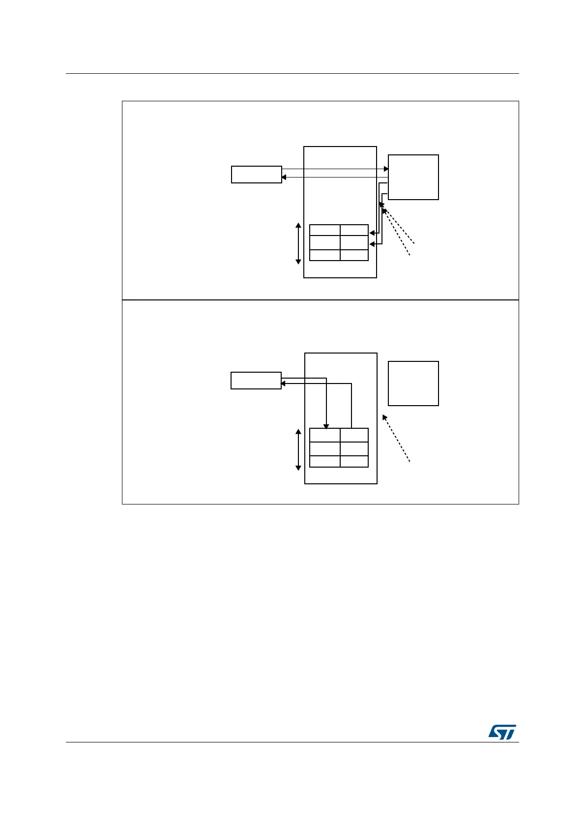
Figure 56. Logic diagram of Read access with RBURST bit set (CAS=1, RPIPE=0)
During a write access or a Precharge command, the read FIFO is flushed and ready to be
filled with new data.
After the first read request, if the current access was not performed to a row boundary, the
SDRAM controller anticipates the next read access during the CAS latency period and the
RPIPE delay (if configured). This is done by incrementing the memory address. The
following condition must be met:
• RBURST control bit should be set to ‘1’ in the FMC_SDCR1 register.
069
$;,0DVWHU
#[
#[
'DWD
'DWD
6'5$0
'HYLFH
&$6
UHDGUHTXHVW#[
'DWD
OLQHV),)2
$GG7DJUHDG),)2
'DWDVWRUHGLQ),)2
LQDGYDQFHGXULQJ
WKH&$6ODWHQF\SHULRG
$GGUHVVPDWFKHVZLWK
RQHRIWKHDGGUHVVWDJV
)0&6'5$0&RQWUROOHU
QG5HDGDFFHVV 5HTXHVWHGGDWDZDVSUHYLRXVO\VWRUHGLQWKH),)2
VW5HDGDFFHVV5HTXHVWHGGDWDLVQRWLQWKH),)2
$;,0DVWHU
#[
#[
'DWD
'DWD
6'5$0
'HYLFH
&$6
UHDGUHTXHVW#[
'DWD
OLQHV),)2
'DWDUHDGIURP),)2
)0&6'5$0&RQWUROOHU
$GG7DJUHDG),)2