RM0390 Rev 4 979/1328
RM0390 Secure digital input/output interface (SDIO)
1031
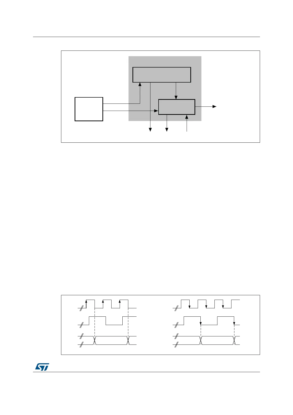
Figure 377. Control unit
The control unit is illustrated in Figure 377. It consists of a power management subunit and
a clock management subunit.
The power management subunit disables the card bus output signals during the power-off
and power-up phases.
The clock management subunit generates and controls the SDIO_CK signal. The SDIO_CK
output can use either the clock divide or the clock bypass mode. The clock output is
inactive:
• after reset
• during the power-off or power-up phases
• if the power saving mode is enabled and the card bus is in the Idle state (eight clock
periods after both the command and data path subunits enter the Idle phase)
The clock management subunit controls SDIO_CK dephasing. When not in bypass mode
the SDIO command and data output are generated on the SDIOCLK falling edge
succeeding the rising edge of SDIO_CK. (SDIO_CK rising edge occurs on SDIOCLK rising
edge) when SDIO_CLKCR[13] bit is reset (NEGEDGE = 0). When SDIO_CLKCR[13] bit is
set (NEGEDGE = 1) SDIO command and data changed on the SDIO_CK falling edge.
When SDIO_CLKCR[10] is set (BYPASS = 1), SDIO_CK rising edge occurs on SDIOCLK
rising edge. The data and the command change on SDIOCLK falling edge whatever
NEGEDGE value.
The data and command responses are latched using SDIO_CK rising edge.
Figure 378. SDIO_CK clock dephasing (BYPASS = 0)
06Y9
&RQWUROXQLW
3RZHUPDQDJHPHQW
&ORFNPDQDJHPHQW
$GDSWHU
UHJLVWHUV
6',2B&.
7RFRPPDQGDQGGDWDSDWK
06Y9
6',2&/.
6',2B&.
1(*('*( 1(*('*(
&0''DWD
RXWSXW