RM0390 Rev 4 95/1328
RM0390 Power controller (PWR)
115
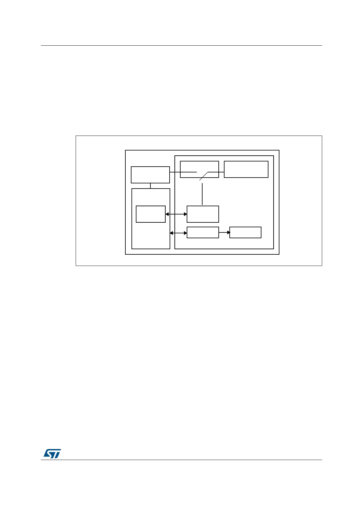
regulator can be ON or OFF depending whether the application needs the backup SRAM
function in Standby and V
BAT
modes or not. The power-down of this regulator is controlled
by a dedicated bit, the BRE control bit of the PWR_CSR register.
The backup SRAM is not mass erased by a tamper event.
When the Flash is read out protected, the backup SRAM is also read protected to prevent
confidential data (such as cryptographic private key) from being accessed. When the
protection level change from level 1 to level 0 is requested, the backup SRAM content is
erased. Refer to the description of Read protection (RDP) option byte.
Figure 9. Backup domain
5.1.3 Voltage regulator
An embedded linear voltage regulator supplies all the digital circuitries except for the backup
domain and the Standby circuitry. The regulator output voltage is around 1.2 V.
This voltage regulator requires two external capacitors to be connected to two dedicated
pins, V
CAP_1
and V
CAP_2
available in all packages. Specific pins must be connected either to
V
SS
or V
DD
to activate or deactivate the voltage regulator. These pins depend on the
package.
When activated by software, the voltage regulator is always enabled after Reset. It works in
three different modes depending on the application modes (Run, Stop, or Standby mode).
• In Run mode, the main regulator supplies full power to the 1.2 V domain (core,
memories and digital peripherals). In this mode, the regulator output voltage (around
1.2 V) can be scaled by software to different voltage values (scale 1, scale 2, and scale
3 can be configured through VOS[1:0] bits of the PWR_CR register). The scale can be
modified only when the PLL is OFF and the HSI or HSE clock source is selected as
system clock source. The new value programmed is active only when the PLL is ON.
When the PLL is OFF, the voltage scale 3 is automatically selected.
The voltage scaling allows optimizing the power consumption when the device is
clocked below the maximum system frequency. After exit from Stop mode, the voltage
069
9ROWDJHUHJXODWRU
!9
9GRPDLQ
%DFNXS65$0
LQWHUIDFH
3RZHUVZLWFK /3YROWDJHUHJXODWRU
!9
%DFNXS65$0
9
57& /6(+]
%DFNXSGRPDLQ