Reset and clock control (RCC) RM0390
138/1328 RM0390 Rev 4
6.3.6 RCC AHB2 peripheral reset register (RCC_AHB2RSTR)
Address offset: 0x14
Reset value: 0x0000 0000
Access: no wait state, word, half-word and byte access
6.3.7 RCC AHB3 peripheral reset register (RCC_AHB3RSTR)
Address offset: 0x18
Reset value: 0x0000 0000
Access: no wait state, word, half-word and byte access.
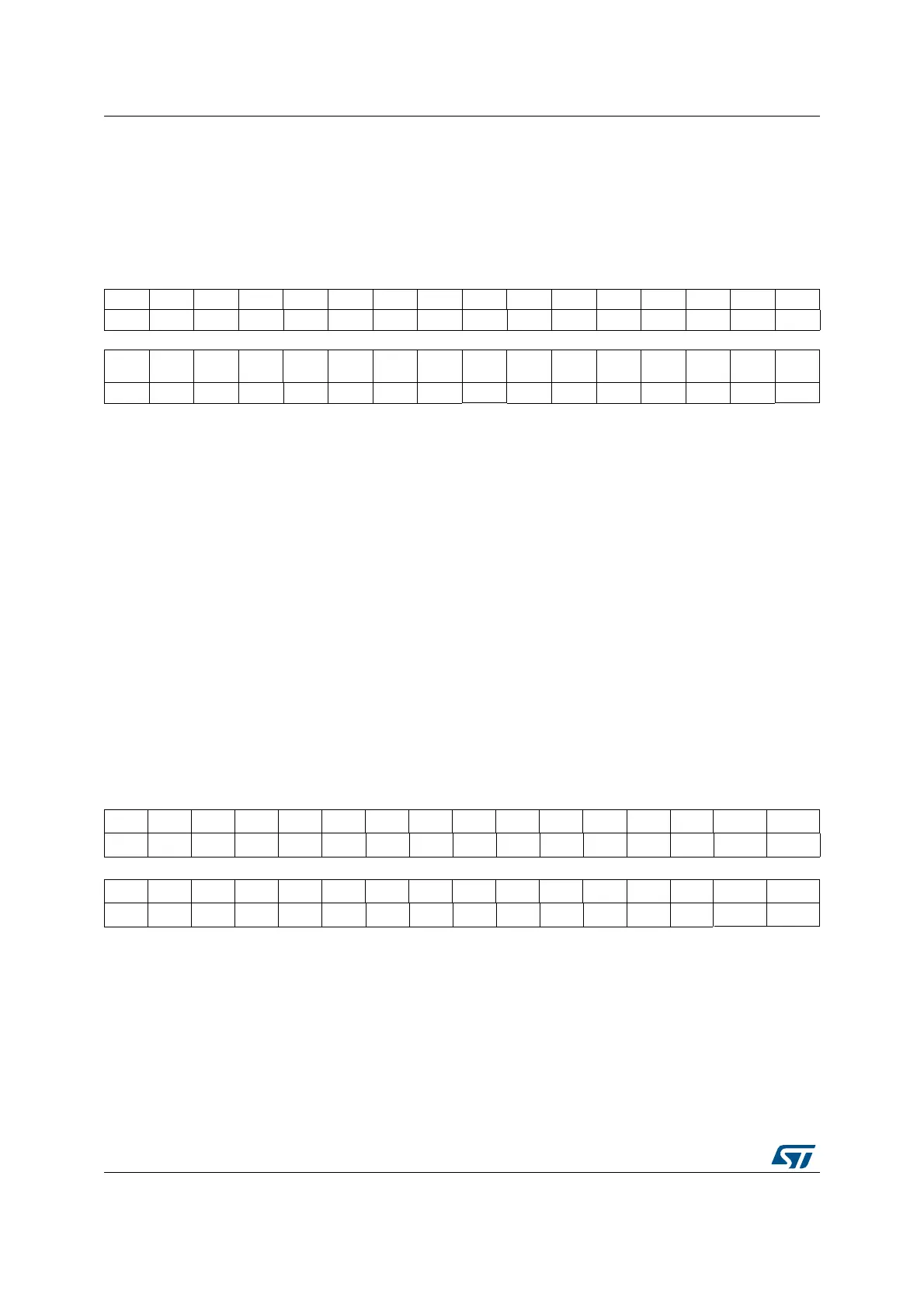
31 30 29 28 27 26 25 24 23 22 21 20 19 18 17 16
Res. Res. Res. Res. Res. Res. Res. Res. Res. Res. Res. Res. Res. Res. Res. Res.
1514131211109876543210
Res. Res. Res. Res. Res. Res. Res. Res.
OTGFS
RST
Res. Res. Res. Res. Res. Res.
DCMI
RST
rw rw
Bits 31:8 Reserved, must be kept at reset value.
Bit 7 OTGFSRST: USB OTG FS module reset
Set and cleared by software.
0: does not reset the USB OTG FS module
1: resets the USB OTG FS module
Bits 6:1 Reserved, must be kept at reset value.
Bit 0 DCMIRST: Camera interface reset
Set and cleared by software.
0: does not reset the Camera interface
1: resets the Camera interface
31 30 29 28 27 26 25 24 23 22 21 20 19 18 17 16
Res. Res. Res. Res. Res. Res. Res. Res. Res. Res. Res. Res. Res. Res. Res. Res.
15141312111098765432 1 0
Res. Res. Res. Res. Res. Res. Res. Res. Res. Res. Res. Res. Res. Res. QSPIRST FMCRST
rw rw
Bits 31:2 Reserved, must be kept at reset value.
Bit 1 QSPIRST: QUADSPI module reset
Set and reset by software
0: does not reset QUADSPI module
1: resets QUADSPI module
 Loading...


