RM0390 Rev 4 1111/1328
RM0390 USB on-the-go full-speed/high-speed (OTG_FS/OTG_HS)
1264
Power and clock gating CSR map
There is a single register for power and clock gating. It is available in both host and device
modes.
31.15 OTG_FS/OTG_HS registers
These registers are available in both host and device modes, and do not need to be
reprogrammed when switching between these modes.
Bit values in the register descriptions are expressed in binary unless otherwise specified.
31.15.1 OTG control and status register (OTG_GOTGCTL)
Address offset: 0x000
Reset value: 0x0001 0000
The OTG_GOTGCTL register controls the behavior and reflects the status of the OTG
function of the core.
... ... ...
Device IN endpoint x
(1)
/Host OUT Channel x
(1)
: DFIFO write access
Device OUT endpoint x
(1)
/Host IN Channel x
(1)
: DFIFO read access
0xX000–0xXFFC
w
r
1. Where x is 5[FS] / 8[HS]in device mode and 11[FS] / 15[HS]in host mode.
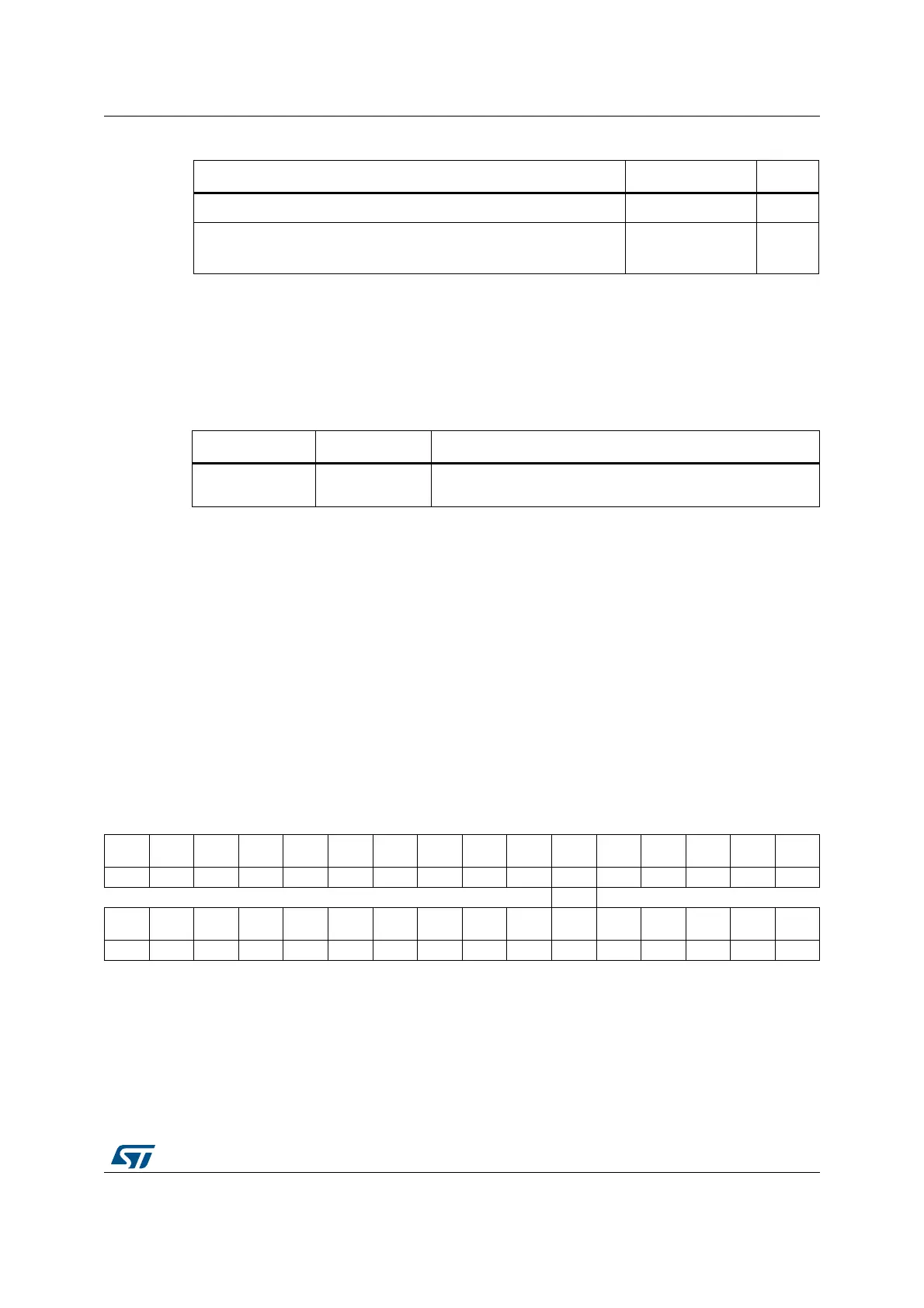
Table 227. Power and clock gating control and status registers
Acronym Offset address Register name
OTG_PCGCCTL 0xE00–0xE04
Section 31.15.60: OTG power and clock gating control
register (OTG_PCGCCTL)
Table 226. Data FIFO (DFIFO) access register map (continued)
FIFO access register section Offset address Access
31 30 29 28 27 26 25 24 23 22 21 20 19 18 17 16
Res. Res. Res. Res. Res. Res. Res. Res. Res. Res.
CUR
MOD
OTG
VER
BSVLD ASVLD DBCT
CID
STS
rrwrrrr
1514131211109876543210
Res. Res. Res. EHEN
DHNP
EN
HSHNP
EN
HNP
RQ
HNG
SCS
BVALO
VAL
BVALO
EN
AVALO
VAL
AVALO
EN
VBVAL
OVAL
VBVAL
OEN
SRQ
SRQ
SCS
rwrwrwrw r rwrwrwrwrwrwrw r