Embedded Flash memory interface RM0390
66/1328 RM0390 Rev 4
3.4 Read interface
3.4.1 Relation between CPU clock frequency and Flash memory read time
To correctly read data from Flash memory, the number of wait states (LATENCY) must be
correctly programmed in the Flash access control register (FLASH_ACR) according to the
frequency of the CPU clock (HCLK) and the supply voltage of the device.
The prefetch buffer must be disabled when the supply voltage is below 2.1 V. The
correspondence between wait states and CPU clock frequency is given in Table 5.
Note: On STM32F446xx devices:
- when VOS[1:0] = '0x01', the maximum value of f
HCLK
is 120 MHz.
- when VOS[1:0] = '0x10', the maximum value of f
HCLK
is 144 MHz. It can be extended to
168 MHz by activating the over-drive mode.
- when VOS[1:0] = '0x11, the maximum value of f
HCLK
is 168 MHz. It can be extended to
180 MHz by activating the over-drive mode. The over-drive mode is not available when V
DD
ranges from 1.8 to 2.1 V (refer to Section 5.1.3: Voltage regulator for details on how to
activate the over-drive mode).
After reset, the CPU clock frequency is 16 MHz and 0 wait state (WS) is configured in the
FLASH_ACR register.
It is highly recommended to use the following software sequences to tune the number of
wait states needed to access the Flash memory with the CPU frequency.
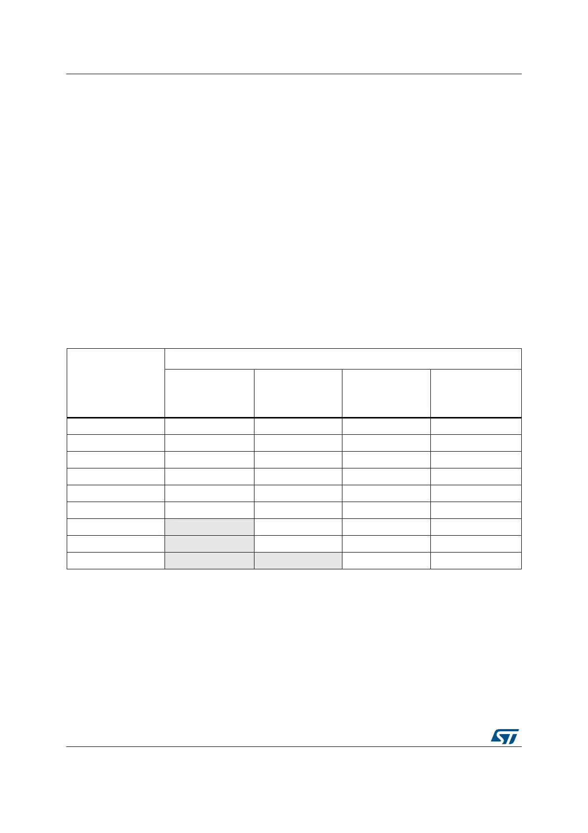
Table 5. Number of wait states according to CPU clock (HCLK) frequency
Wait states (WS)
(LATENCY)
HCLK (MHz)
Voltage range
2.7 V - 3.6 V
Voltage range
2.4 V - 2.7 V
Voltage range
2.1 V - 2.4 V
Voltage range
1.8 V - 2.1 V
Prefetch OFF
0 WS (1 CPU cycle) 0 < HCLK 30 0 <HCLK 24 0 <HCLK 22 0 < HCLK 20
1 WS (2 CPU cycles) 30 < HCLK 60 24 < HCLK 48 22 < HCLK 44 20 < HCLK 40
2 WS (3 CPU cycles) 60 < HCLK 90 48 < HCLK 72 44 < HCLK 66 40 < HCLK 60
3 WS (4 CPU cycles) 90 < HCLK 120 72 < HCLK 96 66 < HCLK 88 60 < HCLK 80
4 WS (5 CPU cycles) 120 < HCLK 150 96 < HCLK 120 88 < HCLK 110 80 < HCLK 100
5 WS (6 CPU cycles) 150 < HCLK 180 120 < HCLK 144 110 < HCLK 132 100 < HCLK 120
6 WS (7 CPU cycles)
144 < HCLK 168 132 < HCLK 154 120 < HCLK 140
7 WS (8 CPU cycles)
168 <HCLK 180 154 <HCLK 176 140 < HCLK 160
8 WS (9 CPU cycles)
176 <HCLK 180 160 < HCLK 168