Serial peripheral interface/ inter-IC sound (SPI/I2S) RM0390
848/1328 RM0390 Rev 4
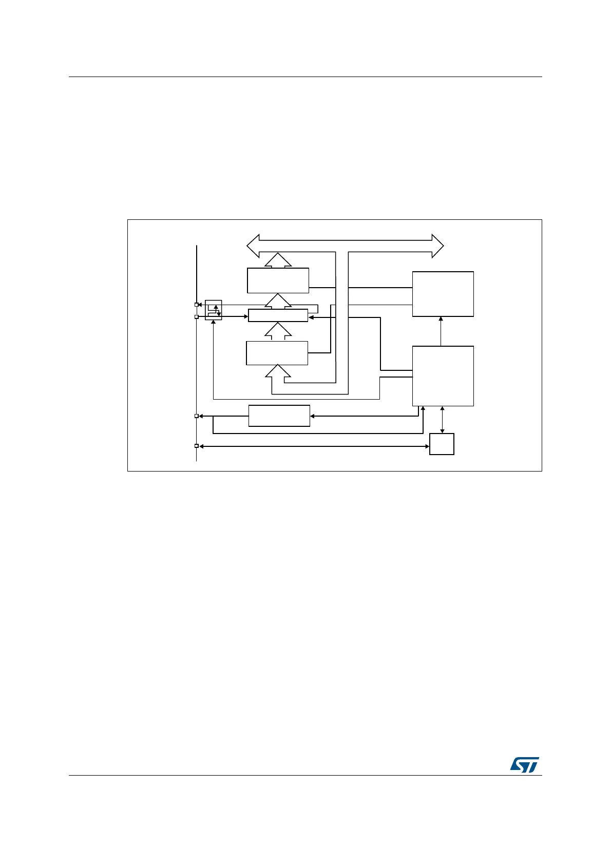
26.3 SPI functional description
26.3.1 General description
The SPI allows synchronous, serial communication between the MCU and external devices.
Application software can manage the communication by polling the status flag or using
dedicated SPI interrupt. The main elements of SPI and their interactions are shown in the
following block diagram Figure 304.
Figure 304. SPI block diagram
Four I/O pins are dedicated to SPI communication with external devices.
• MISO: Master In / Slave Out data. In the general case, this pin is used to transmit data
in slave mode and receive data in master mode.
• MOSI: Master Out / Slave In data. In the general case, this pin is used to transmit data
in master mode and receive data in slave mode.
• SCK: Serial Clock output pin for SPI masters and input pin for SPI slaves.
• NSS: Slave select pin. Depending on the SPI and NSS settings, this pin can be used to
either:
– select an individual slave device for communication
– synchronize the data frame or
– detect a conflict between multiple masters
See Section 26.3.5: Slave select (NSS) pin management for details.
The SPI bus allows the communication between one master device and one or more slave
devices. The bus consists of at least two wires - one for the clock signal and the other for
synchronous data transfer. Other signals can be added depending on the data exchange
between SPI nodes and their slave select signal management.
06Y9
6KLIWUHJLVWHU
:ULWH
5HDG
&RPPXQLFDWLRQ
FRQWUROOHU
$GGUHVVDQGGDWDEXV
&5&FRQWUROOHU
,QWHUQDO166
&5&(1
&5&1(;7
/6%),567
&32/
&3+$
'))
026,
0,62
6&.
166
5[
EXIIHU
7;
EXIIHU
%5>@
%,',2(
%,',02'(
5;2/1<
166
ORJLF
%DXGUDWH
JHQHUDWRU