USB on-the-go full-speed/high-speed (OTG_FS/OTG_HS) RM0390
1136/1328 RM0390 Rev 4
Device mode
31.15.11 OTG non-periodic transmit FIFO/queue status register
(OTG_HNPTXSTS)
Address offset: 0x02C
Reset value: 0x0008 0200 for USB OTG FS
Reset value: 0x0008 0400 for USB OTG HS
Note: In device mode, this register is not valid.
This read-only register contains the free space information for the non-periodic Tx FIFO and
the non-periodic transmit request queue.
Bits 31:16 TX0FD: Endpoint 0 Tx FIFO depth
This value is in terms of 32-bit words.
Minimum value is 16
Programmed values must respect the available FIFO memory allocation and must not
exceed the power-on value.
Bits 15:0 TX0FSA: Endpoint 0 transmit RAM start address
This field configures the memory start address for the endpoint 0 transmit FIFO RAM.
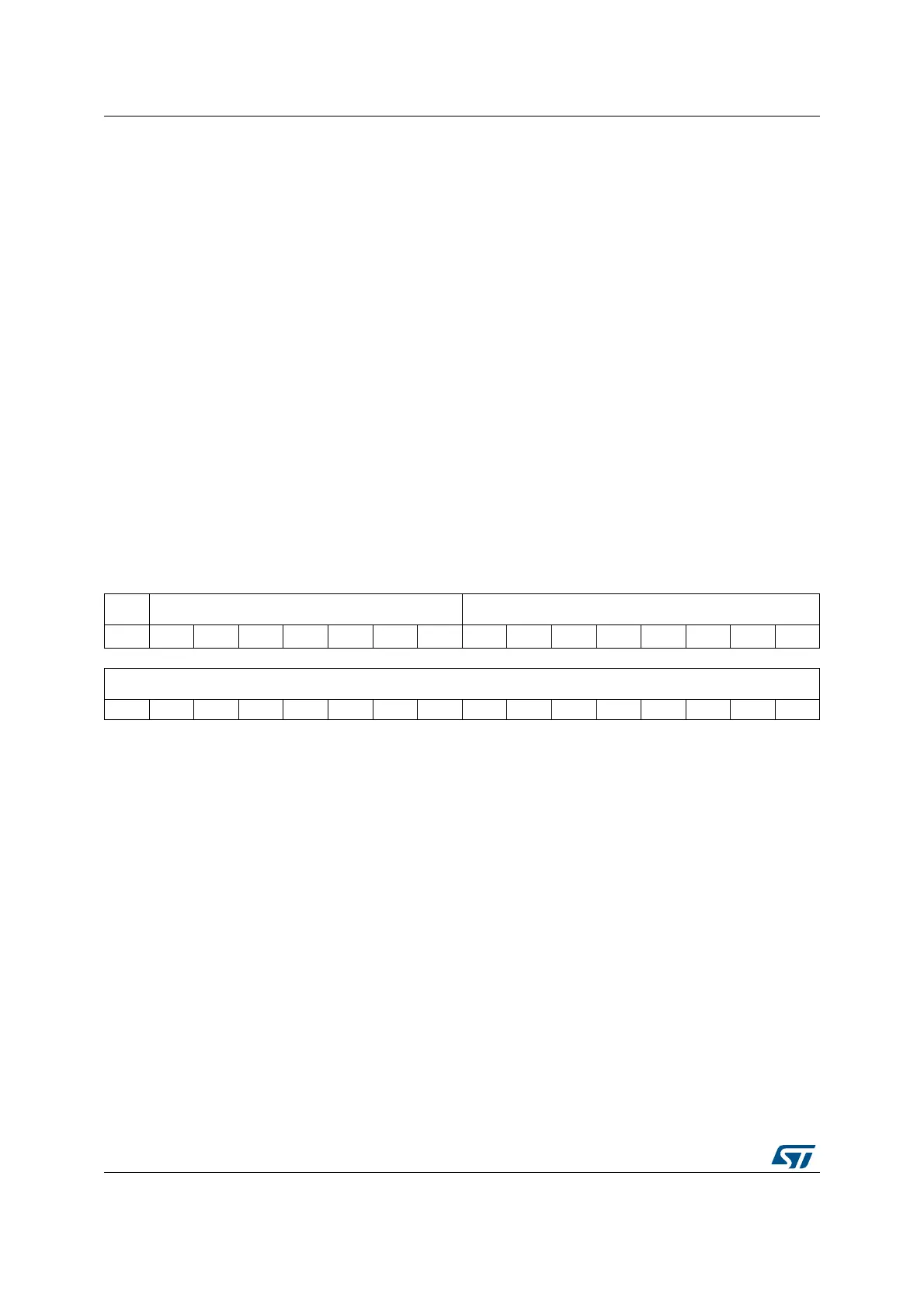
31 30 29 28 27 26 25 24 23 22 21 20 19 18 17 16
Res. NPTXQTOP[6:0] NPTQXSAV[7:0]
rrrrrrrrrrrrrrr
1514131211109876543210
NPTXFSAV[15:0]
rrrrrrrrrrrrrrrr
 Loading...


