Flexible memory controller (FMC) RM0390
260/1328 RM0390 Rev 4
11.5.1 External memory interface signals
Table 49, Table 50 and Table 5 1 list the signals that are typically used to interface with NOR
Flash memory, SRAM and PSRAM.
Note: The prefix “N” identifies the signals that are active low.
NOR Flash memory, non-multiplexed I/Os
The maximum capacity is 512 Mbits (26 address lines).
NOR Flash memory, 16-bit multiplexed I/Os
The maximum capacity is 512 Mbits.
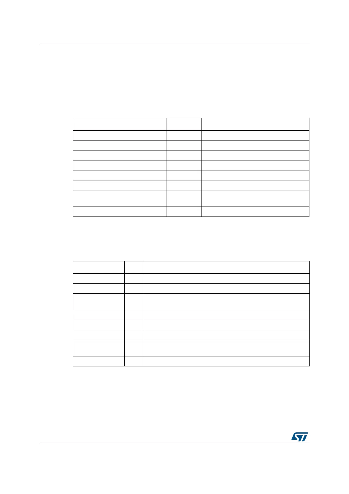
Table 49. Non-multiplexed I/O NOR Flash memory
FMC signal name I/O Function
CLK O Clock (for synchronous access)
A[25:0] O Address bus
D[15:0] I/O Bidirectional data bus
NE[x] O Chip Select, x = 1..4
NOE O Output enable
NWE O Write enable
NL(=NADV) O
Latch enable (this signal is called address
valid, NADV, by some NOR Flash devices)
NWAIT I NOR Flash wait input signal to the FMC
Table 50. 16-bit multiplexed I/O NOR Flash memory
FMC signal name I/O Function
CLK O Clock (for synchronous access)
A[25:16] O Address bus
AD[15:0] I/O
16-bit multiplexed, bidirectional address/data bus (the 16-bit address
A[15:0] and data D[15:0] are multiplexed on the databus)
NE[x] O Chip Select, x = 1..4
NOE O Output enable
NWE O Write enable
NL(=NADV) O
Latch enable (this signal is called address valid, NADV, by some NOR
Flash devices)
NWAIT I NOR Flash wait input signal to the FMC
 Loading...


