Serial peripheral interface/ inter-IC sound (SPI/I2S) RM0390
880/1328 RM0390 Rev 4
26.6.5 I
2
S master mode
The I
2
S can be configured in master mode. This means that the serial clock is generated on
the CK pin as well as the Word Select signal WS. Master clock (MCK) may be output or not,
controlled by the MCKOE bit in the SPIx_I2SPR register.
Procedure
1. Select the I2SDIV[7:0] bits in the SPIx_I2SPR register to define the serial clock baud
rate to reach the proper audio sample frequency. The ODD bit in the SPIx_I2SPR
register also has to be defined.
2. Select the CKPOL bit to define the steady level for the communication clock. Set the
MCKOE bit in the SPIx_I2SPR register if the master clock MCK needs to be provided
to the external ADC audio component (the I2SDIV and ODD values should be
computed depending on the state of the MCK output, for more details refer to
Section 26.6.4: Clock generator).
3. Set the I2SMOD bit in the SPIx_I2SCFGR register to activate the I
2
S functions and
choose the I
2
S standard through the I2SSTD[1:0] and PCMSYNC bits, the data length
through the DATLEN[1:0] bits and the number of bits per channel by configuring the
CHLEN bit. Select also the I
2
S master mode and direction (Transmitter or Receiver)
through the I2SCFG[1:0] bits in the SPIx_I2SCFGR register.
4. If needed, select all the potential interrupt sources and the DMA capabilities by writing
the SPIx_CR2 register.
5. The I2SE bit in SPIx_I2SCFGR register must be set.
WS and CK are configured in output mode. MCK is also an output, if the MCKOE bit in
SPIx_I2SPR is set.
Transmission sequence
The transmission sequence begins when a half-word is written into the Tx buffer.
Lets assume the first data written into the Tx buffer corresponds to the left channel data.
When data are transferred from the Tx buffer to the shift register, TXE is set and data
corresponding to the right channel have to be written into the Tx buffer. The CHSIDE flag
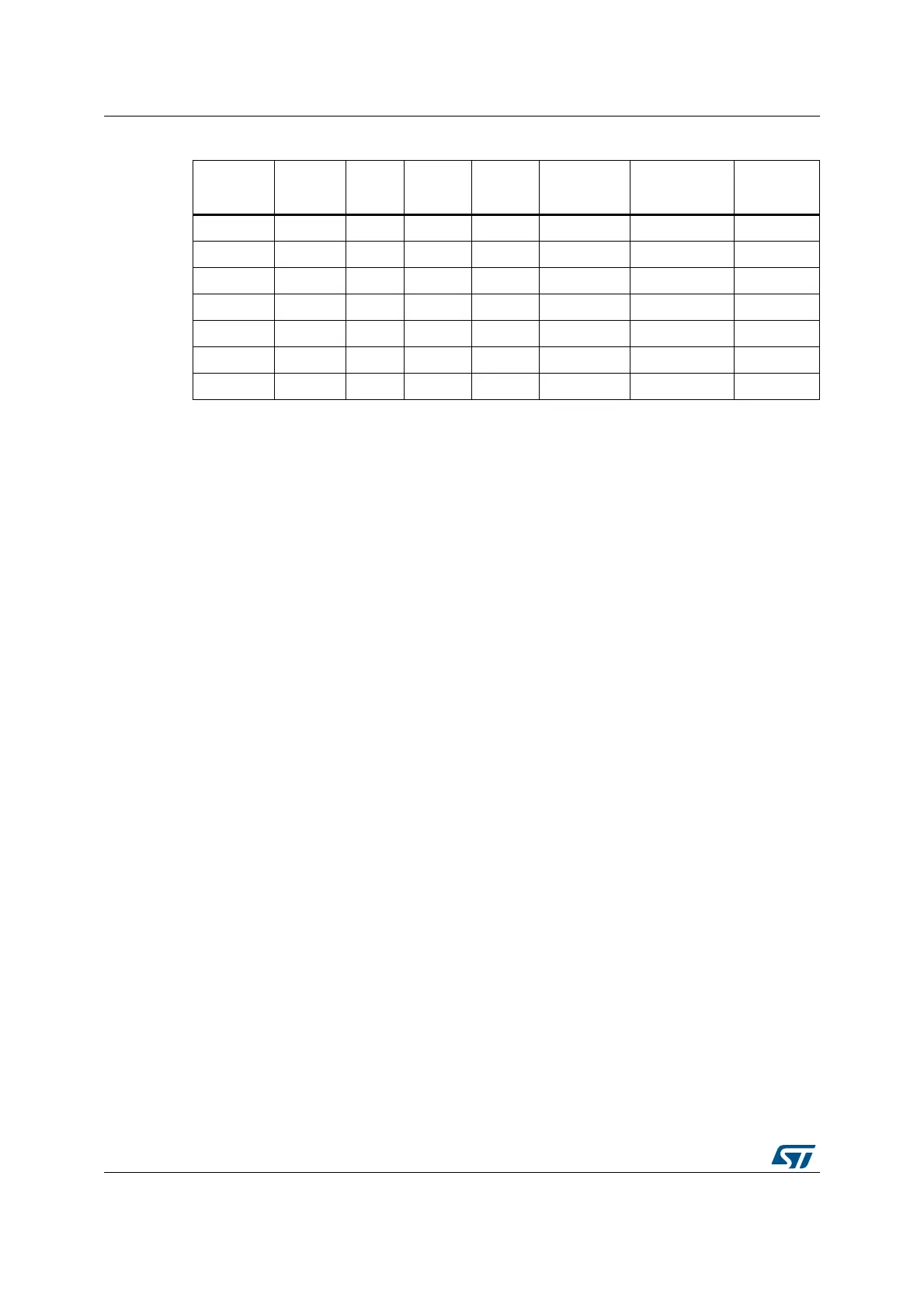
48 32 4 1 Yes 22050 20833.333 5.5178%
48 16 6 0 Yes 16000 15625 2.3438%
48 32 6 0 Yes 16000 15625 2.3438%
48 16 8 1 Yes 11025 11029.4118 0.0400%
48 32 8 1 Yes 11025 11029.4118 0.0400%
48 16 11 1 Yes 8000 8152.17391 1.9022%
48 32 11 1 Yes 8000 8152.17391 1.9022%
1. This table gives only example values for different clock configurations. Other configurations allowing
optimum clock precision are possible.
Table 164. Audio-frequency precision using standard 8 MHz HSE
(1)
(continued)
SYSCLK
(MHz)
Data
length
I2SDIV I2SODD MCLK
Target f
S
(Hz)
Real f
S
(KHz) Error
 Loading...


