RM0390 Rev 4 231/1328
RM0390 Direct memory access controller (DMA)
237
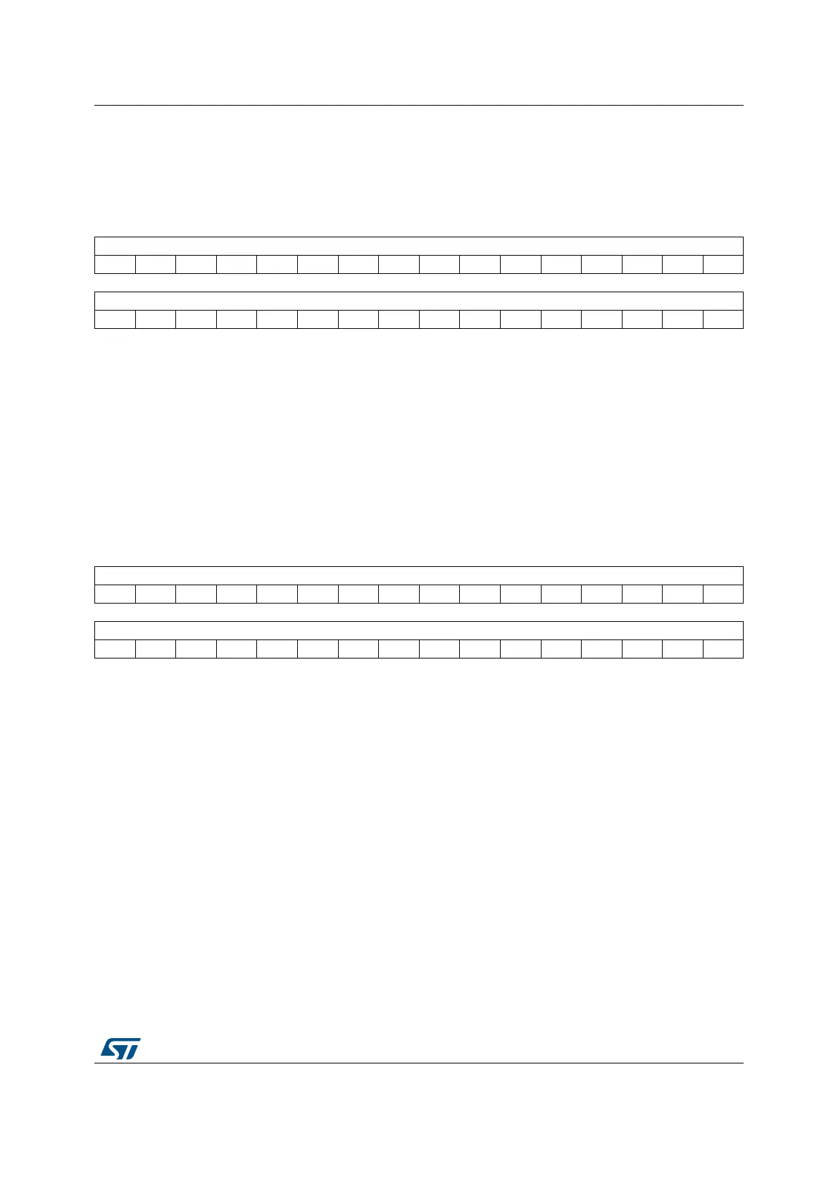
9.5.7 DMA stream x peripheral address register (DMA_SxPAR) (x = 0..7)
Address offset: 0x18 + 0x18 * stream number
Reset value: 0x0000 0000
9.5.8 DMA stream x memory 0 address register
(DMA_SxM0AR) (x = 0..7)
Address offset: 0x1C + 0x18 * stream number
Reset value: 0x0000 0000
31 30 29 28 27 26 25 24 23 22 21 20 19 18 17 16
PAR[31:16]
rw rw rw rw rw rw rw rw rw rw rw rw rw rw rw rw
1514131211109876543210
PAR[15:0]
rw rw rw rw rw rw rw rw rw rw rw rw rw rw rw rw
Bits 31:0 PAR[31:0]: peripheral address
Base address of the peripheral data register from/to which the data is read/written.
These bits are write-protected and can be written only when bit EN = '0' in the DMA_SxCR
register.
31 30 29 28 27 26 25 24 23 22 21 20 19 18 17 16
M0A[31:16]
rw rw rw rw rw rw rw rw rw rw rw rw rw rw rw rw
1514131211109876543210
M0A[15:0]
rw rw rw rw rw rw rw rw rw rw rw rw rw rw rw rw
Bits 31:0 M0A[31:0]: memory 0 address
Base address of memory area 0 from/to which the data is read/written.
These bits are write-protected. They can be written only if:
– the stream is disabled (bit EN= '0' in the DMA_SxCR register) or
– the stream is enabled (EN=’1’ in DMA_SxCR register) and bit CT = '1' in the
DMA_SxCR register (in double-buffer mode).