Direct memory access controller (DMA) RM0390
214/1328 RM0390 Rev 4
Note: Peripheral port may be the source or the destination (it could also be the memory source in
the case of memory-to-memory transfer).
PSIZE, MSIZE and NDT[15:0] have to be configured so as to ensure that the last transfer
will not be incomplete. This can occur when the data width of the peripheral port (PSIZE
bits) is lower than the data width of the memory port (MSIZE bits). This constraint is
summarized in Table 33.
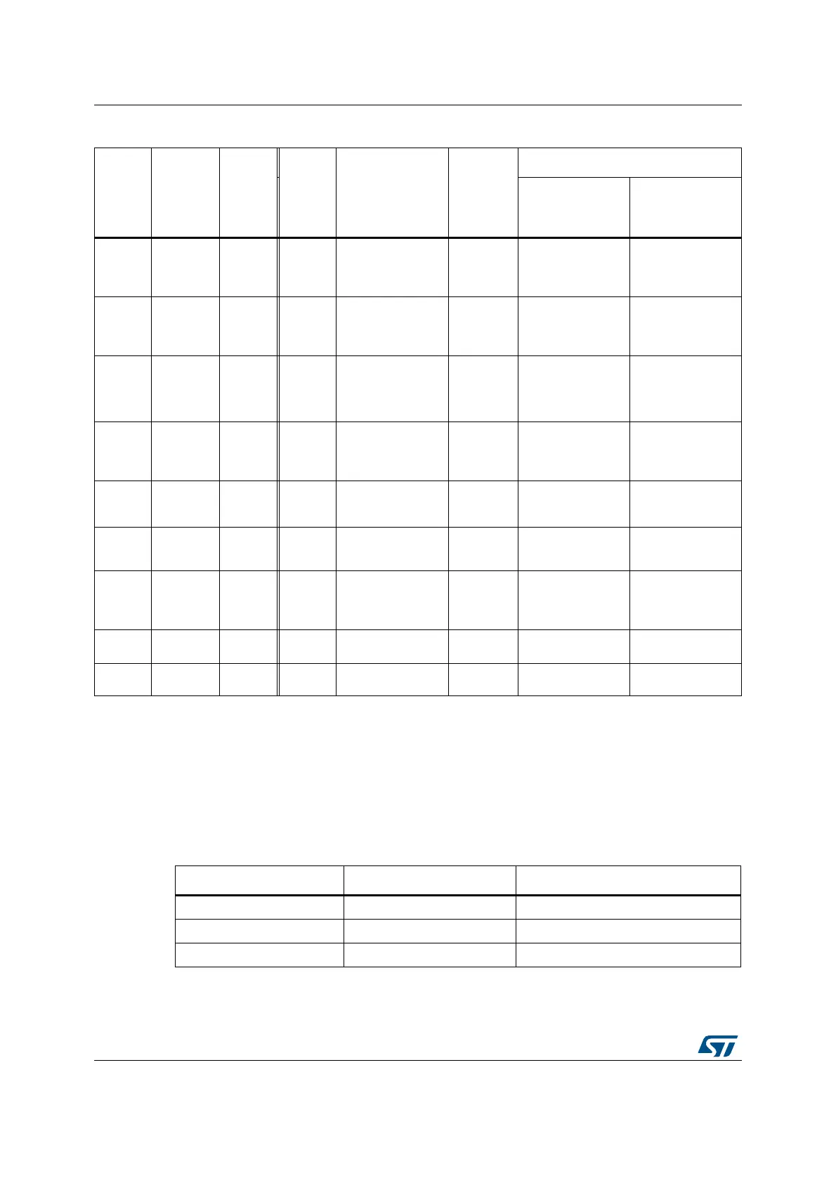
Table 32. Packing/unpacking and endian behavior (bit PINC = MINC = 1)
AHB
memory
port
width
AHB
peripheral
port
width
Number
of data
items to
transfer
(NDT)
Memory
transfer
number
Memory port
address / byte
lane
Peripheral
transfer
number
Peripheral port address / byte lane
PINCOS = 1 PINCOS = 0
884
1
2
3
4
0x0 / B0[7:0]
0x1 / B1[7:0]
0x2 / B2[7:0]
0x3 / B3[7:0]
1
2
3
4
0x0 / B0[7:0]
0x4 / B1[7:0]
0x8 / B2[7:0]
0xC / B3[7:0]
0x0 / B0[7:0]
0x1 / B1[7:0]
0x2 / B2[7:0]
0x3 / B3[7:0]
8162
1
2
3
4
0x0 / B0[7:0]
0x1 / B1[7:0]
0x2 / B2[7:0]
0x3 / B3[7:0]
1
2
0x0 / B1|B0[15:0]
0x4 / B3|B2[15:0]
0x0 / B1|B0[15:0]
0x2 / B3|B2[15:0]
8321
1
2
3
4
0x0 / B0[7:0]
0x1 / B1[7:0]
0x2 / B2[7:0]
0x3 / B3[7:0]
1
0x0 /
B3|B2|B1|B0[31:0]
0x0 /
B3|B2|B1|B0[31:0]
16 8 4
1
2
0x0 / B1|B0[15:0]
0x2 / B3|B2[15:0]
1
2
3
4
0x0 / B0[7:0]
0x4 / B1[7:0]
0x8 / B2[7:0]
0xC / B3[7:0]
0x0 / B0[7:0]
0x1 / B1[7:0]
0x2 / B2[7:0]
0x3 / B3[7:0]
16 16 2
1
2
0x0 / B1|B0[15:0]
0x2 / B1|B0[15:0]
1
2
0x0 / B1|B0[15:0]
0x4 / B3|B2[15:0]
0x0 / B1|B0[15:0]
0x2 / B3|B2[15:0]
16 32 1
1
2
0x0 / B1|B0[15:0]
0x2 / B3|B2[15:0]
1
0x0 /
B3|B2|B1|B0[31:0]
0x0 /
B3|B2|B1|B0[31:0]
32 8 4
1
0x0 / B3|B2|B1|B0[31:0]
1
2
3
4
0x0 / B0[7:0]
0x4 / B1[7:0]
0x8 / B2[7:0]
0xC / B3[7:0]
0x0 / B0[7:0]
0x1 / B1[7:0]
0x2 / B2[7:0]
0x3 / B3[7:0]
32 16 2
1
0x0 /B3|B2|B1|B0[31:0]
1
2
0x0 / B1|B0[15:0]
0x4 / B3|B2[15:0]
0x0 / B1|B0[15:0]
0x2 / B3|B2[15:0]
32 32 1 1 0x0 /B3|B2|B1|B0 [31:0] 1
0x0 /B3|B2|B1|B0
[31:0]
0x0 /
B3|B2|B1|B0[31:0]
Table 33. Restriction on NDT versus PSIZE and MSIZE
PSIZE[1:0] of DMA_SxCR MSIZE[1:0] of DMA_SxCR NDT[15:0] of DMA_SxNDTR
00 (8-bit) 01 (16-bit) must be a multiple of 2
00 (8-bit) 10 (32-bit) must be a multiple of 4
01 (16-bit) 10 (32-bit) must be a multiple of 2
 Loading...


