Digital camera interface (DCMI) RM0390
424/1328 RM0390 Rev 4
15.4 DCMI functional overview
The digital camera interface is a synchronous parallel interface that can receive high-speed
(up to 54 Mbytes/s) data flows. It consists of up to 14 data lines (D13-D0) and a pixel clock
line (DCMI_PIXCLK). The pixel clock has a programmable polarity, so that data can be
captured on either the rising or the falling edge of the pixel clock.
The data are packed into a 32-bit data register (DCMI_DR) and then transferred through a
general-purpose DMA channel. The image buffer is managed by the DMA, not by the
camera interface.
The data received from the camera can be organized in lines/frames (raw YUB/RGB/Bayer
modes) or can be a sequence of JPEG images. To enable JPEG image reception, the JPEG
bit (bit 3 of DCMI_CR register) must be set.
The data flow is synchronized either by hardware using the optional DCMI_HSYNC
(horizontal synchronization) and DCMI_VSYNC (vertical synchronization) signals or by
synchronization codes embedded in the data flow.
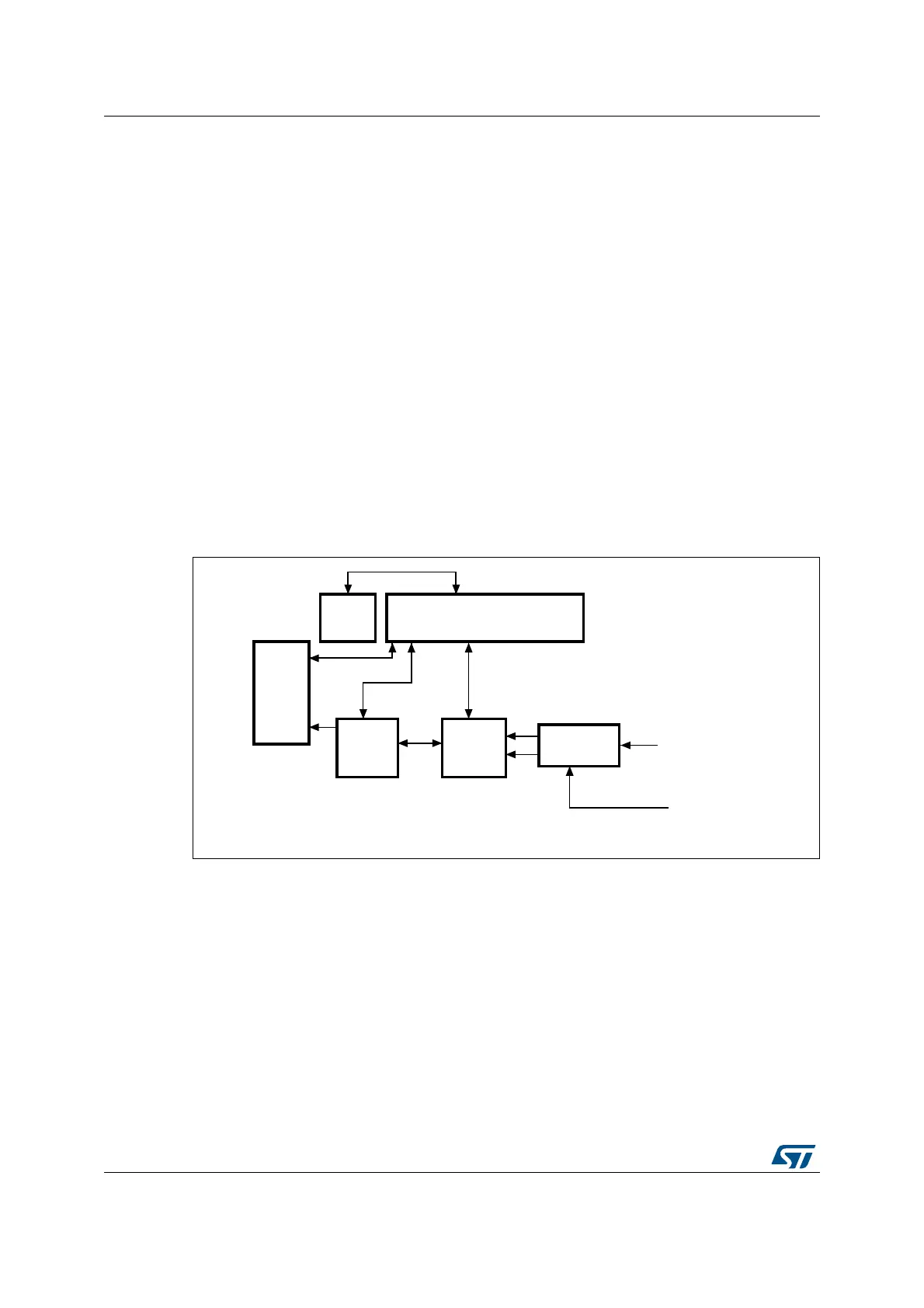
15.4.1 DCMI block diagram
Figure 101 shows the DCMI block diagram.
Figure 101. DCMI block diagram
'0$
LQWHUIDFH
&RQWURO6WDWXV
UHJLVWHU
$+%
LQWHUIDFH
),)2
'DWD
IRUPDWWHU
'DWD
H[WUDFWLRQ
6\QFKURQL]HU
'&0,B3,;&/.
'&0,B'>@'&0,B+6<1&'&0,B96<1&
DLE