RM0390 Rev 4 427/1328
RM0390 Digital camera interface (DCMI)
448
12-bit data
When EDM[1:0] in DCMI_CR are programmed to “10”, the camera interface captures the
12-bit data at its input DCMI_D[0..11] and stores them as the 12 least significant bits of a 16-
bit word. The remaining most significant bits are cleared to zero. So, in this case a 32-bit
data word is made up every two pixel clock cycles.
The first captured data are placed in the LSB position in the 32-bit word and the 2
nd
captured data are placed in the MSB position in the 32-bit word as shown in Table 99.
14-bit data
When EDM[1:0] in DCMI_CR are programmed to “11”, the camera interface captures the
14-bit data at its input DCMI_D[0..13] and stores them as the 14 least significant bits of a 16-
bit word. The remaining most significant bits are cleared to zero. So, in this case a 32-bit
data word is made up every two pixel clock cycles.
The first captured data are placed in the LSB position in the 32-bit word and the 2
nd
captured data are placed in the MSB position in the 32-bit word as shown in Table 100.
15.4.4 Synchronization
The digital camera interface supports embedded or hardware (DCMI_HSYNC and
DCMI_VSYNC) synchronization. When embedded synchronization is used, it is up to the
digital camera module to make sure that the 0x00 and 0xFF values are used ONLY for
synchronization (not in data). Embedded synchronization codes are supported only for the
8-bit parallel data interface width (that is, in the DCMI_CR register, the EDM[1:0] bits should
be cleared to “00”).
For compressed data, the DCMI supports only the hardware synchronization mode. In this
case, DCMI_VSYNC is used as a start/end of the image, and DCMI_HSYNC is used as a
Data Valid signal. Figure 104 shows the corresponding timing diagram.
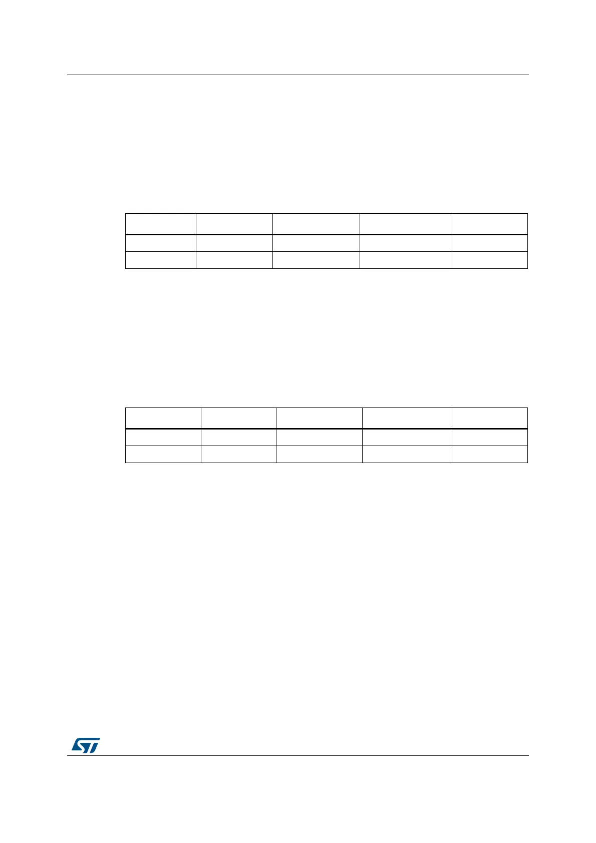
Table 99. Positioning of captured data bytes in 32-bit words (12-bit width)
Byte address 31:28 27:16 15:12 11:0
00D
n+1
[11:0] 0 D
n
[11:0]
40D
n+3
[11:0] 0 D
n+2
[11:0]
Table 100. Positioning of captured data bytes in 32-bit words (14-bit width)
Byte address 31:30 29:16 15:14 13:0
00D
n+1
[13:0] 0 D
n
[13:0]
40D
n+3
[13:0] 0 D
n+2
[13:0]
 Loading...


