RM0390 Rev 4 257/1328
RM0390 Flexible memory controller (FMC)
324
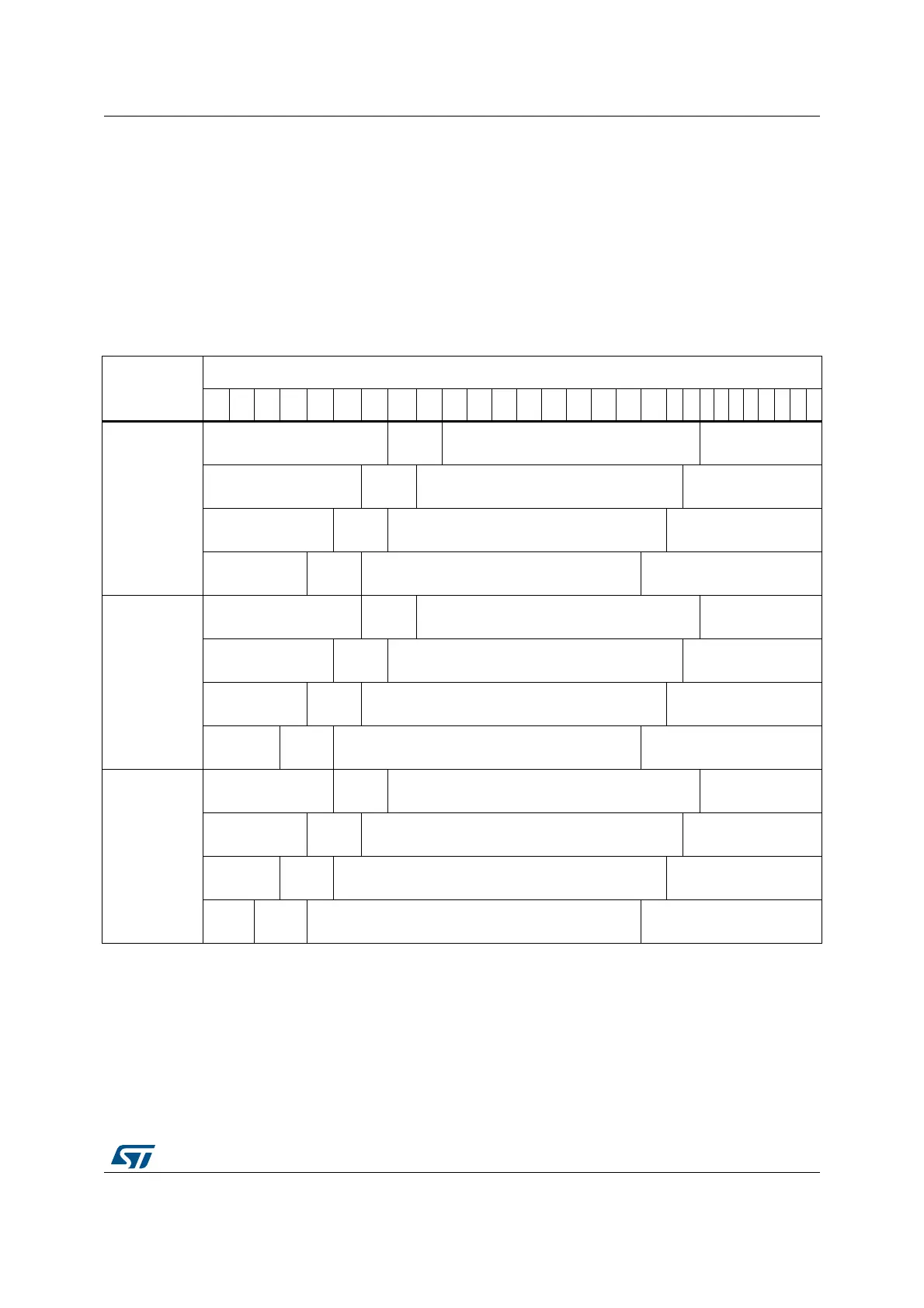
The HADDR[27:0] bits are translated to external SDRAM address depending on the
SDRAM controller configuration:
• Data size:8 or 16 bits
• Row size:11, 12 or 13 bits
• Column size: 8, 9, 10 or 11 bits
• Number of internal banks: two or four internal banks
The following tables show the SDRAM address mapping versus the SDRAM controller
configuration.
Table 46. SDRAM address mapping with 8-bit data bus width
(1)(2)
Row size
configuration
HADDR(AHB Internal Address Lines)
27 26 25 24 23 22 21 20 19 18 17 16 15 14 13 12 11 10 9 8 76543210
11-bit row size
configuration
Res.
Bank
[1:0]
Row[10:0] Column[7:0]
Res.
Bank
[1:0]
Row[10:0] Column[8:0]
Res.
Bank
[1:0]
Row[10:0] Column[9:0]
Res.
Bank
[1:0]
Row[10:0] Column[10:0]
12-bit row size
configuration
Res.
Bank
[1:0]
Row[11:0] Column[7:0]
Res.
Bank
[1:0]
Row[11:0] Column[8:0]
Res.
Bank
[1:0]
Row[11:0] Column[9:0]
Res.
Bank
[1:0]
Row[11:0] Column[10:0]
13-bit row size
configuration
Res.
Bank
[1:0]
Row[12:0] Column[7:0]
Res.
Bank
[1:0]
Row[12:0] Column[8:0]
Res.
Bank
[1:0]
Row[12:0] Column[9:0]
Res.
Bank
[1:0]
Row[12:0] Column[10:0]
1. BANK[1:0] are the Bank Address BA[1:0]. When only 2 internal banks are used, BA1 must always be set to ‘0’.
2. Access to Reserved (Res.) address range generates an AHB error.
 Loading...


