Advanced-control timers (TIM1&TIM8) RM0390
478/1328 RM0390 Rev 4
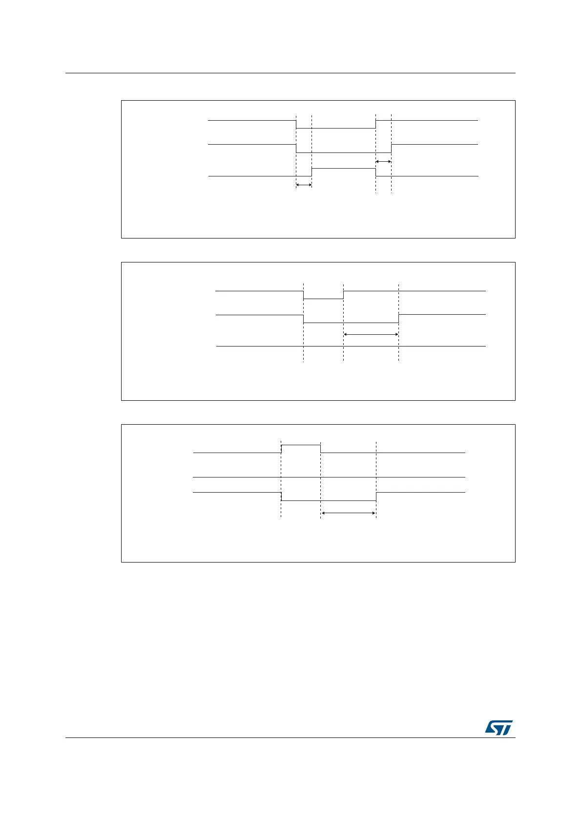
Figure 144. Complementary output with dead-time insertion.
Figure 145. Dead-time waveforms with delay greater than the negative pulse.
Figure 146. Dead-time waveforms with delay greater than the positive pulse.
The dead-time delay is the same for each of the channels and is programmable with the
DTG bits in the TIMx_BDTR register. Refer to Section 16.4.18: TIM1&TIM8 break and dead-
time register (TIMx_BDTR) for delay calculation.
Re-directing OCxREF to OCx or OCxN
In output mode (forced, output compare or PWM), OCxREF can be re-directed to the OCx
output or to OCxN output by configuring the CCxE and CCxNE bits in the TIMx_CCER
register.
This allows you to send a specific waveform (such as PWM or static active level) on one
output while the complementary remains at its inactive level. Other alternative possibilities
GHOD\
GHOD\
2&[5()
2&[
2&[1
069
069
GHOD\
2&[5()
2&[
2&[1
069
GHOD\
2&[5()
2&[
2&[1