Device electronic signature RM0390
1318/1328 RM0390 Rev 4
Address offset: 0x08
Read only = 0xXXXX XXXX, where X is factory-programmed
34.2 Flash memory size register
Base address: 0x1FFF 7A22
Address offset: 0x00
Read only = 0xXXXX, where X is factory-programmed
34.3 Package data register
Base address: 0x1FFF7BF0
Address offset: 0x00
Read only = 0xXXXX, where X is factory-programmed
31 30 29 28 27 26 25 24 23 22 21 20 19 18 17 16
U_ID[95:80]
rrrrrrrrrrrrrrrr
15 14 13 12 11 10 9 8 7 6 5 4 3 2 1 0
U_ID[79:64]
rrrrrrrrrrrrrrrr
Bits 31:0 U_ID[95:64]: 95:64 Unique ID bits.
1514131211109876543210
F_SIZE
rrrrrrrrrrrrrrrr
Bits 15:0 F_SIZE[15:0]: Flash memory size
Indicates the size of the device Flash memory, expressed in KBytes.
As an example, 0x0200 corresponds to 512 KBytes.
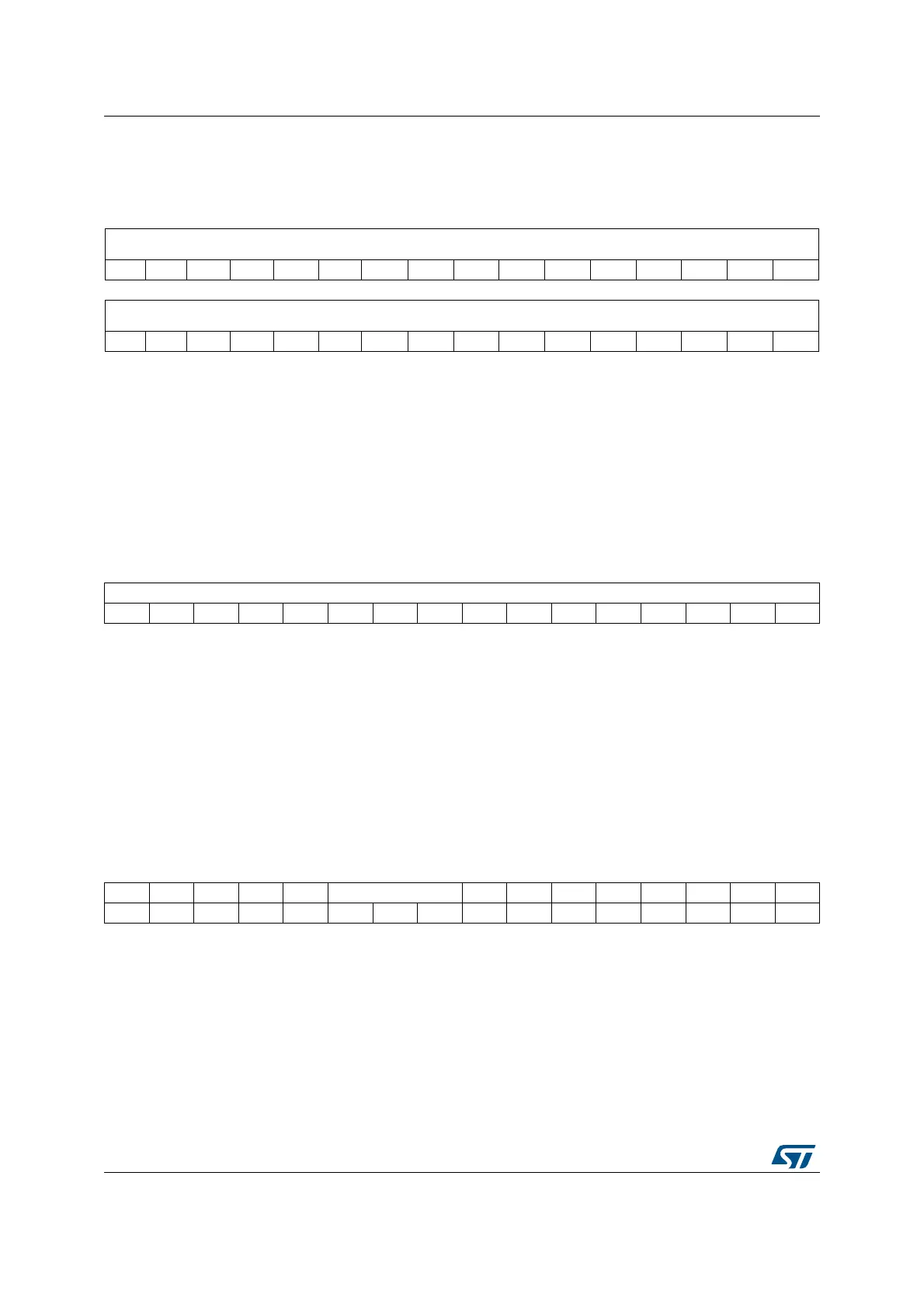
1514131211109876543210
Res. Res. Res. Res. Res. PKG[2:0] Res. Res. Res. Res. Res. Res. Res. Res.
rrr
Bits 15:11 Reserved, must be kept at reset value
Bits 10:8 PKG[2:0]: Package type
0x011: LQFP144, UFBGA144 (7x7) and UFBGA144 (10x10) packages
0x010: WLCSP81 package
0x001: LQFP100 package
0x000: LQFP64 package
Bits 7:0 Reserved, must be kept at reset value.
 Loading...


