RM0390 Rev 4 255/1328
RM0390 Flexible memory controller (FMC)
324
11.4.1 NOR/PSRAM address mapping
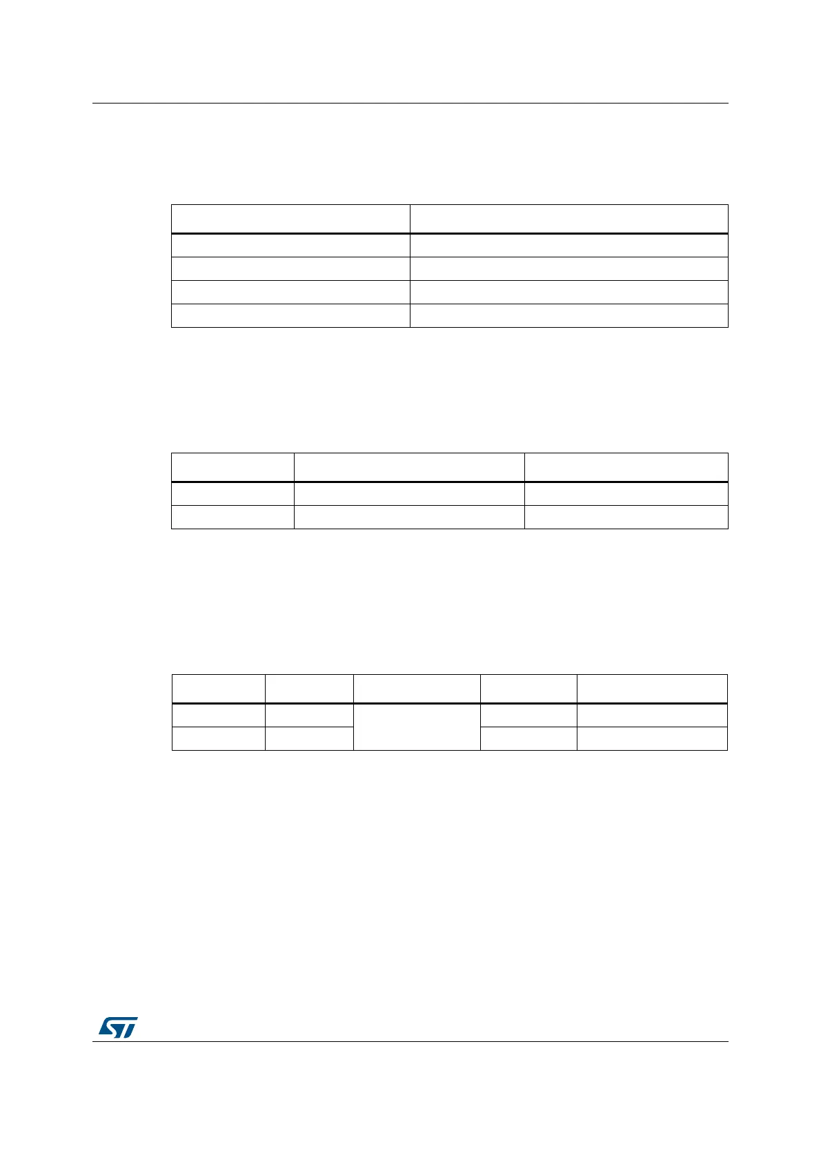
HADDR[27:26] bits are used to select one of the four memory banks as shown in Table 40.
The HADDR[25:0] bits contain the external memory address. Since HADDR is a byte
address whereas the memory is addressed at word level, the address actually issued to the
memory varies according to the memory data width, as shown in the following table.
11.4.2 NAND Flash memory address mapping
The NAND bank is divided into memory areas as indicated in Table 42.
For NAND Flash memory, the common and attribute memory spaces are subdivided into
three sections (see in Table 43 below) located in the lower 256 Kbytes:
• Data section (first 64 Kbytes in the common/attribute memory space)
• Command section (second 64 Kbytes in the common / attribute memory space)
• Address section (next 128 Kbytes in the common / attribute memory space)
Table 40. NOR/PSRAM bank selection
HADDR[27:26]
(1)
1. HADDR are internal AHB address lines that are translated to external memory.
Selected bank
00 Bank 1 - NOR/PSRAM 1
01 Bank 1 - NOR/PSRAM 2
10 Bank 1 - NOR/PSRAM 3
11 Bank 1 - NOR/PSRAM 4
Table 41. NOR/PSRAM External memory address
Memory width
(1)
1. In case of a 16-bit external memory width, the FMC will internally use HADDR[25:1] to generate the
address for external memory FMC_A[24:0].
Whatever the external memory width, FMC_A[0] should be connected to external memory address A[0].
Data address issued to the memory Maximum memory capacity (bits)
8-bit HADDR[25:0] 64 Mbytes x 8 = 512 Mbit
16-bit HADDR[25:1] >> 1 64 Mbytes/2 x 16 = 512 Mbit
Table 42. NAND memory mapping and timing registers
Start address End address FMC bank Memory space Timing register
0x8800 0000 0x8BFF FFFF
Bank 3 - NAND Flash
Attribute FMC_PATT (0x8C)
0x8000 0000 0x83FF FFFF Common FMC_PMEM (0x88)