RM0390 Rev 4 339/1328
RM0390 Quad-SPI interface (QUADSPI)
353
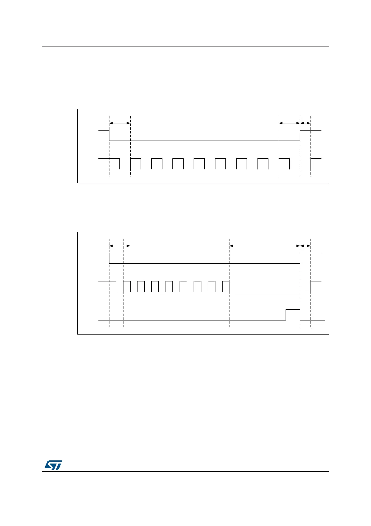
When CKMODE = 1 (“mode3”) and DDRM = 1 (DDR mode), nCS falls one CLK cycle
before an operation first rising CLK edge, and nCS rises one CLK cycle after the operation
final active rising CLK edge, as shown in Figure 67. Because DDR operations must finish
with a falling edge, CLK is low when nCS rises, and CLK rises back up one half of a CLK
cycle afterwards.
Figure 67. nCS when CKMODE = 1 in DDR mode (T = CLK period)
When the FIFO stays full in a read operation or if the FIFO stays empty in a write operation,
the operation stalls and CLK stays low until firmware services the FIFO. If an abort occurs
when an operation is stalled, nCS rises just after the abort is requested and then CLK rises
one half of a CLK cycle later, as shown in Figure 68.
Figure 68. nCS when CKMODE = 1 with an abort (T = CLK period)
When not in dual-flash mode (DFM = 0), only FLASH 1 is accessed and thus the BK2_nCS
stays high. In dual-flash mode, BK2_nCS behaves exactly the same as BK1_nCS. Thus, if
there is a FLASH 2 and if the application always stays in dual-flash mode, then FLASH 2
may use BK1_nCS and the pin outputting BK2_nCS can be used for other functions.
069
Q&6
6&/.
&ORFNVWDOOHG7 7
$ERUW