RM0390 Rev 4 261/1328
RM0390 Flexible memory controller (FMC)
324
PSRAM/SRAM, non-multiplexed I/Os
The maximum capacity is 512 Mbits.
PSRAM, 16-bit multiplexed I/Os
The maximum capacity is 512 Mbits (26 address lines).
11.5.2 Supported memories and transactions
Table 53 below shows an example of the supported devices, access modes and
transactions when the memory data bus is 16-bit wide for NOR Flash memory, PSRAM and
SRAM. The transactions not allowed (or not supported) by the FMC are shown in gray in
this example.
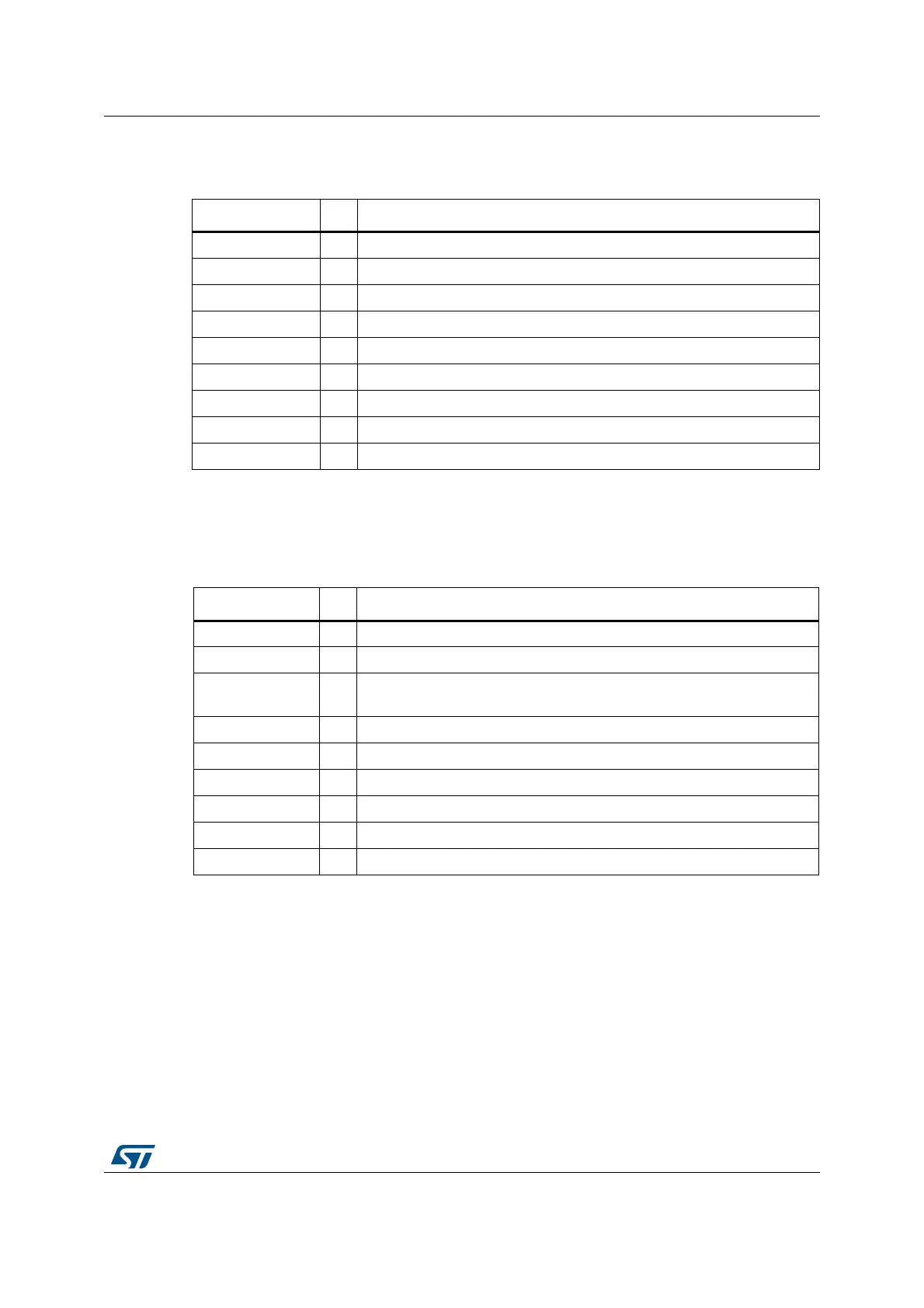
Table 51. Non-multiplexed I/Os PSRAM/SRAM
FMC signal name I/O Function
CLK O Clock (only for PSRAM synchronous access)
A[25:0] O Address bus
D[15:0] I/O Data bidirectional bus
NE[x] O Chip Select, x = 1..4 (called NCE by PSRAM (CellularRAM™ i.e. CRAM))
NOE O Output enable
NWE O Write enable
NL(= NADV) O Address valid only for PSRAM input (memory signal name: NADV)
NWAIT I PSRAM wait input signal to the FMC
NBL[1:0] O Byte lane output. Byte 0 and Byte 1 control (upper and lower byte enable)
Table 52. 16-Bit multiplexed I/O PSRAM
FMC signal name I/O Function
CLK O Clock (for synchronous access)
A[25:16] O Address bus
AD[15:0] I/O
16-bit multiplexed, bidirectional address/data bus (the 16-bit address
A[15:0] and data D[15:0] are multiplexed on the databus)
NE[x] O Chip Select, x = 1..4 (called NCE by PSRAM (CellularRAM™ i.e. CRAM))
NOE O Output enable
NWE O Write enable
NL(= NADV) O Address valid PSRAM input (memory signal name: NADV)
NWAIT I PSRAM wait input signal to the FMC
NBL[1:0] O Byte lane output. Byte 0 and Byte 1 control (upper and lower byte enable)