RM0390 Rev 4 115/1328
RM0390 Power controller (PWR)
115
5.5 PWR register map
The following table summarizes the PWR registers.
Refer to Table 1 on page 57 for the register boundary addresses.
Bit 3 BRR: Backup regulator ready
Set by hardware to indicate that the Backup Regulator is ready.
0: Backup Regulator not ready
1: Backup Regulator ready
Note: This bit is not reset when the device wakes up from Standby mode or by a system reset
or power reset.
Bit 2 PVDO: PVD output
This bit is set and cleared by hardware. It is valid only if PVD is enabled by the PVDE bit.
0: V
DD
is higher than the PVD threshold selected with the PLS[2:0] bits.
1: V
DD
is lower than the PVD threshold selected with the PLS[2:0] bits.
Note: The PVD is stopped by Standby mode. For this reason, this bit is equal to 0 after
Standby or reset until the PVDE bit is set.
Bit 1 SBF: Standby flag
This bit is set by hardware and cleared only by a POR/PDR (power-on reset/power-down
reset) or by setting the CSBF bit in the PWR power control register (PWR_CR)
0: Device has not been in Standby mode
1: Device has been in Standby mode
Bit 0 WUF: Wakeup flag
This bit is set by hardware and cleared either by a system reset or by setting the CWUF bit in
the PWR_CR register.
0: No wakeup event occurred
1: A wakeup event was received from the WKUP pin or from the RTC alarm (Alarm A or
Alarm B), RTC Tamper event, RTC TimeStamp event or RTC Wakeup).
Note: An additional wakeup event is detected if the WKUP pin is enabled (by setting the
EWUP bit) when the WKUP pin level is already high.
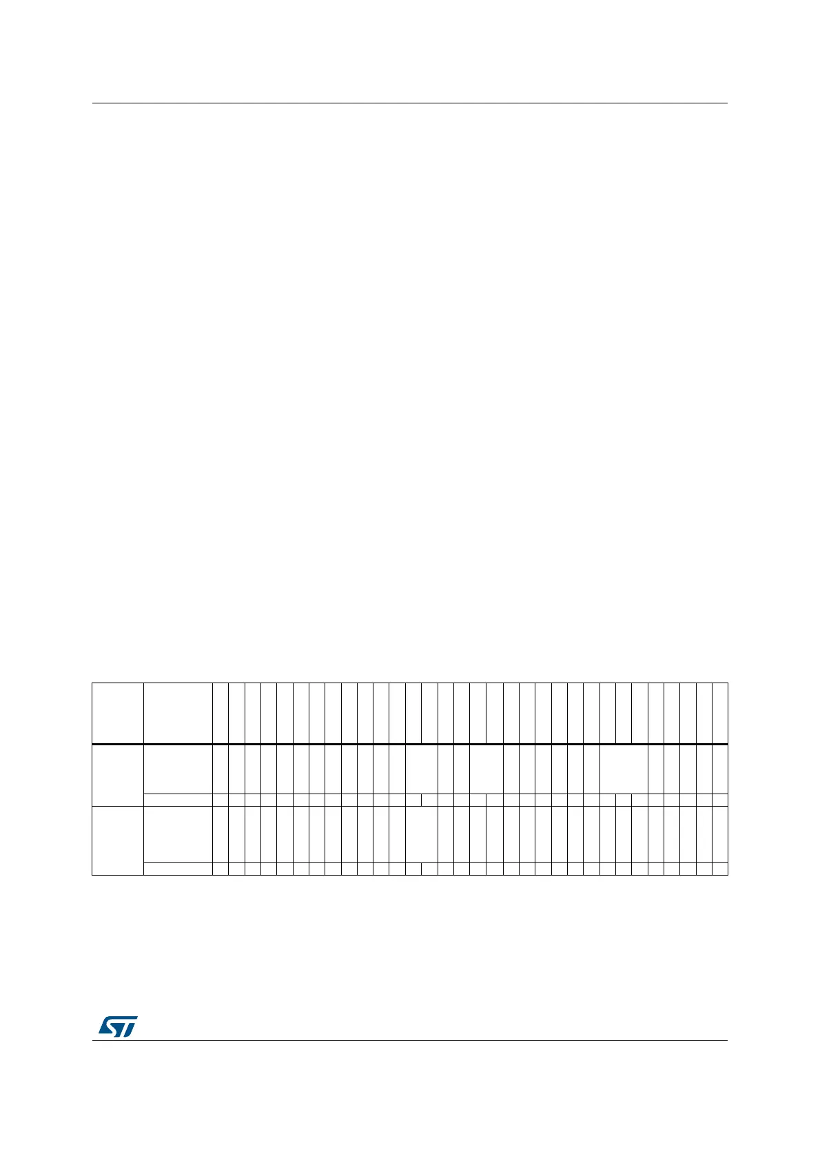
Table 20. PWR - register map and reset values
Offset Register
31
30
29
28
27
26
25
24
23
22
21
20
19
18
17
16
15
14
13
12
11
10
9
8
7
6
5
4
3
2
1
0
0x000
PWR_CR
Res.
Res.
Res.
Res.
Res.
Res.
Res.
Res.
Res.
Res.
FISSR
FMSSR
UDEN[1:0]
ODSWEN
ODEN
VOS[1:0]
ADCDC1
Res.
MRUDS
LPUDS
FPDS
DBP
PLS[2:0]
PVDE
CSBF
CWUF
PDDS
LPDS
Reset value 000000110 000000000000
0x004
PWR_CSR
Res.
Res.
Res.
Res.
Res.
Res.
Res.
Res.
Res.
Res.
Res.
Res.
UDRDY[1:0]
ODSWRDY
ODRDY
Res.
VOSRDY
Res.
Res.
Res.
Res.
BRE
EWUP1
EWUP2.
Res.
Res.
Res.
BRR
PVDO
SBF
WUF
Reset value 0000 0 000 0000