Reset and clock control (RCC) RM0390
170/1328 RM0390 Rev 4
6.3.27 RCC dedicated clocks configuration register 2 (DCKCFGR2)
Address offset: 0x94
Reset value: 0x0000 0000
Access: no wait state, word, half-word and byte access.
This register allows to enable or disable the clock gating for the specified IPs.
Bit 4
SRAM_CKEN: SRQAM controller clock enable
0: the clock gating is enabled
1: the clock gating is disabled, the clock is always enabled.
Bit 3
SPARE_CKEN: Spare clock enable
0: the clock gating is enabled
1: the clock gating is disabled, the clock is always enabled.
Bit 2
CM4DBG_CKEN: Cortex M4 ETM clock enable
0: the clock gating is enabled
1: the clock gating is disabled, the clock is always enabled.
Bit 1
AHB2APB2_CKEN: AHB to APB2 Bridge clock enable
0: the clock gating is enabled
1: the clock gating is disabled, the clock is always enabled.
Bit 0
AHB2APB1_CKEN: AHB to APB1 Bridge clock enable
0: the clock gating is enabled
1: the clock gating is disabled, the clock is always enabled.
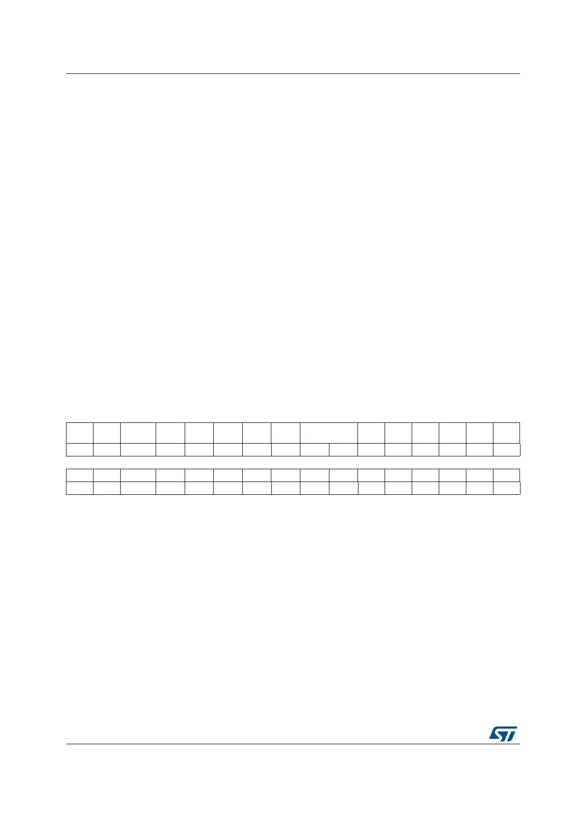
31 30 29 28 27 26 25 24 23 22 21 20 19 18 17 16
Res. Res.
SPDIFRX
SEL
SDIO
SEL
CK48M
SEL
CEC
SEL
Res. Res.
FMPI2C1SEL
[1:0]
Res. Res. Res. Res. Res. Res.
rw rw rw rw rw rw
151413 1211109 8 7 6 543210
Res. Res. Res. Res. Res. Res. Res. Res. Res. Res. Res. Res. Res. Res. Res. Res.
Bits 31:30 Reserved, must be kept at reset value.
Bit 29
SPDIFRXSEL: SPDIF-Rx clock selection
1: f
(PLLI2S_P)
0: f
(PLL_R)
Bit 28
SDIOSEL: SDIO clock selection
1: Clock System
0: Clock 48 MHz
Bit 27
CK48MSEL: SDIO/USBFS/HS clock selection
1: f
(PLLSAI_P)
0: f
(PLL_Q)
Bit 26
CECSEL: HDMI CEC clock source selection
1: LSE
0: HSI/488