Reset and clock control (RCC) RM0390
136/1328 RM0390 Rev 4
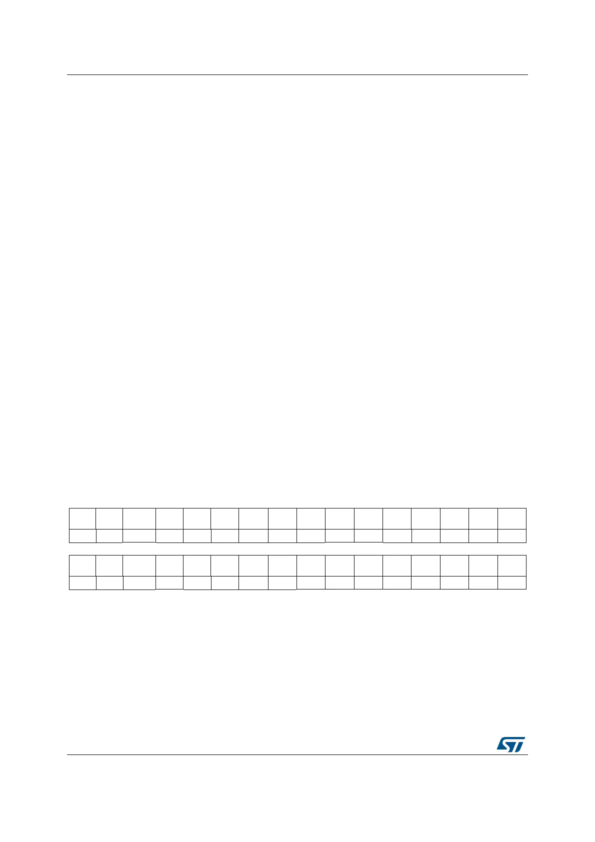
6.3.5 RCC AHB1 peripheral reset register (RCC_AHB1RSTR)
Address offset: 0x10
Reset value: 0x0000 0000
Access: no wait state, word, half-word and byte access.
Bit 3 HSERDYF: HSE ready interrupt flag
This bit is set by hardware when External High Speed clock becomes stable and
HSERDYDIE is set.
It is cleared by software by setting the HSERDYC bit.
0: No clock ready interrupt caused by the HSE oscillator
1: Clock ready interrupt caused by the HSE oscillator
Bit 2 HSIRDYF: HSI ready interrupt flag
This bit is set by hardware when the Internal High Speed clock becomes stable and
HSIRDYDIE is set.
It is cleared by software by setting the HSIRDYC bit.
0: No clock ready interrupt caused by the HSI oscillator
1: Clock ready interrupt caused by the HSI oscillator
Bit 1 LSERDYF: LSE ready interrupt flag
This bit is set by hardware when the External Low Speed clock becomes stable and
LSERDYDIE is set.
It is cleared by software by setting the LSERDYC bit.
0: No clock ready interrupt caused by the LSE oscillator
1: Clock ready interrupt caused by the LSE oscillator
Bit 0 LSIRDYF: LSI ready interrupt flag
This bit is set by hardware when the internal low speed clock becomes stable and
LSIRDYDIE is set.
It is cleared by software by setting the LSIRDYC bit.
0: No clock ready interrupt caused by the LSI oscillator
1: Clock ready interrupt caused by the LSI oscillator
31 30 29 28 27 26 25 24 23 22 21 20 19 18 17 16
Res. Res.
OTGHS
RST
Res. Res. Res. Res Res. Res.
DMA2
RST
DMA1
RST
Res. Res. Res. Res. Res.
rw rw rw
15 14 13 12 11 10 9 8 7 6 5 4 3 2 1 0
Res. Res. Res.
CRC
RST
Res. Res. Res. Res.
GPIOH
RST
GPIOG
RST
GPIOF
RST
GPIOE
RST
GPIOD
RST
GPIOC
RST
GPIOB
RST
GPIOA
RST
rw rw rw rw rw rw rw rw rw
Bits 31:30 Reserved, must be kept at reset value.
Bit 29 OTGHSRST: USB OTG HS module reset
This bit is set and cleared by software.
0: does not reset the USB OTG HS module
1: resets the USB OTG HS module
Bits 28:23 Reserved, must be kept at reset value.