Flexible memory controller (FMC) RM0390
294/1328 RM0390 Rev 4
11.6 NAND Flash controller
The FMC generates the appropriate signal timings to drive the following types of device:
• 8- and 16-bit NAND Flash memories
The NAND bank is configured through dedicated registers (Section 11.6.7). The
programmable memory parameters include access timings (shown in Table 74) and ECC
configuration.
11.6.1 External memory interface signals
The following tables list the signals that are typically used to interface NAND Flash memory.
Note: The prefix “N” identifies the signals which are active low.
8-bit NAND Flash memory
Bits 3:0 ADDSET[3:0]: Address setup phase duration.
These bits are written by software to define the duration of the address setup phase in HCLK
cycles (refer to Figure 34 to Figure 46), used in asynchronous accesses:
0000: ADDSET phase duration = 0 × HCLK clock cycle
...
1111: ADDSET phase duration = 15 × HCLK clock cycles (default value after reset)
Note: In synchronous accesses, this value is not used, the address setup phase is always 1 Flash
clock period duration. In muxed mode, the minimum ADDSET value is 1.
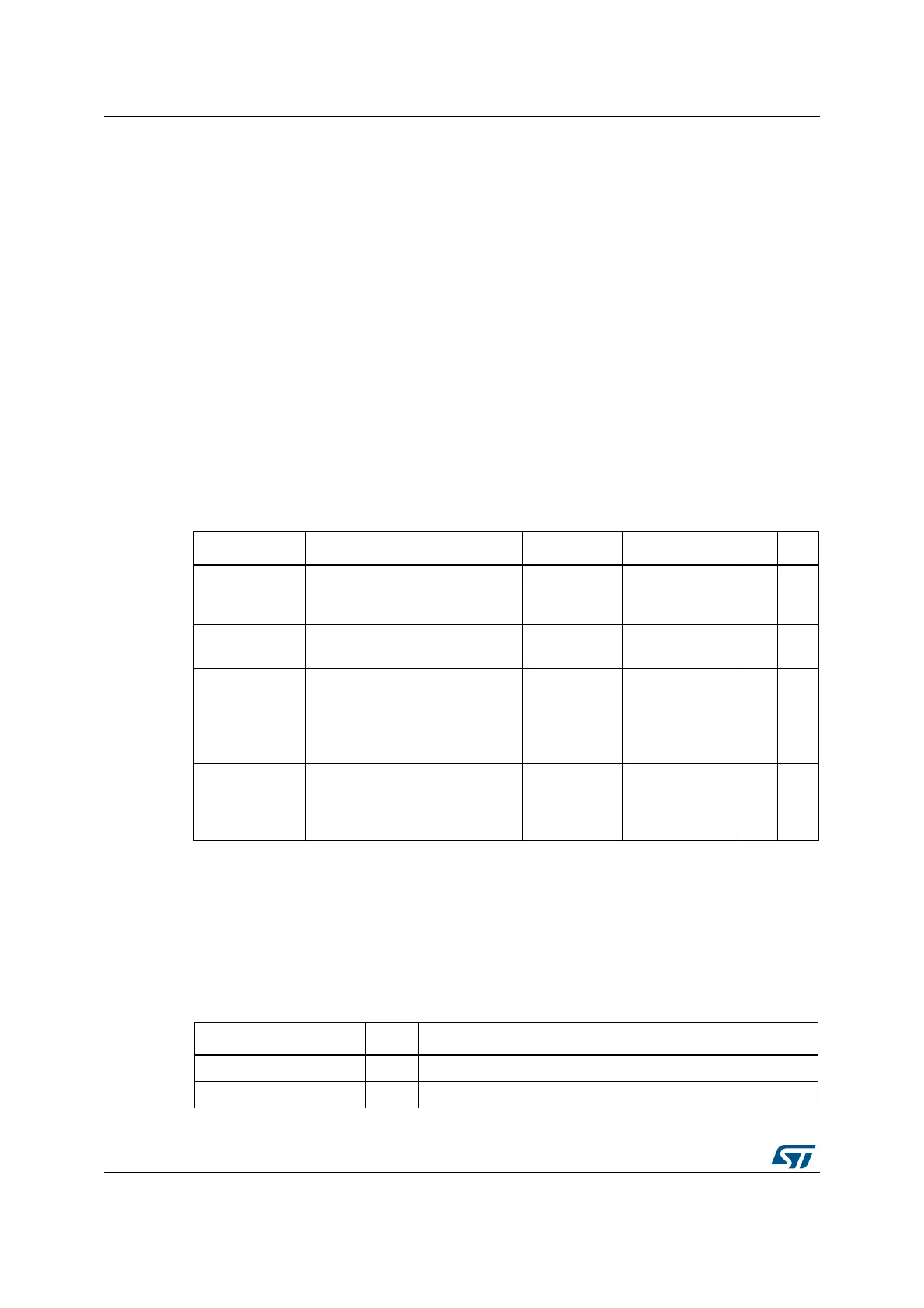
Table 74. Programmable NAND Flash access parameters
Parameter Function Access mode Unit Min. Max.
Memory setup
time
Number of clock cycles (HCLK)
required to set up the address
before the command assertion
Read/Write
AHB clock cycle
(HCLK)
1 255
Memory wait
Minimum duration (in HCLK clock
cycles) of the command assertion
Read/Write
AHB clock cycle
(HCLK)
2 255
Memory hold
Number of clock cycles (HCLK)
during which the address must be
held (as well as the data if a write
access is performed) after the
command de-assertion
Read/Write
AHB clock cycle
(HCLK)
1 254
Memory
databus high-Z
Number of clock cycles (HCLK)
during which the data bus is kept
in high-Z state after a write
access has started
Write
AHB clock cycle
(HCLK)
1 255
Table 75. 8-bit NAND Flash
FMC signal name I/O Function
A[17] O NAND Flash address latch enable (ALE) signal
A[16] O NAND Flash command latch enable (CLE) signal