Serial audio interface (SAI) RM0390
932/1328 RM0390 Rev 4
28.3 SAI functional description
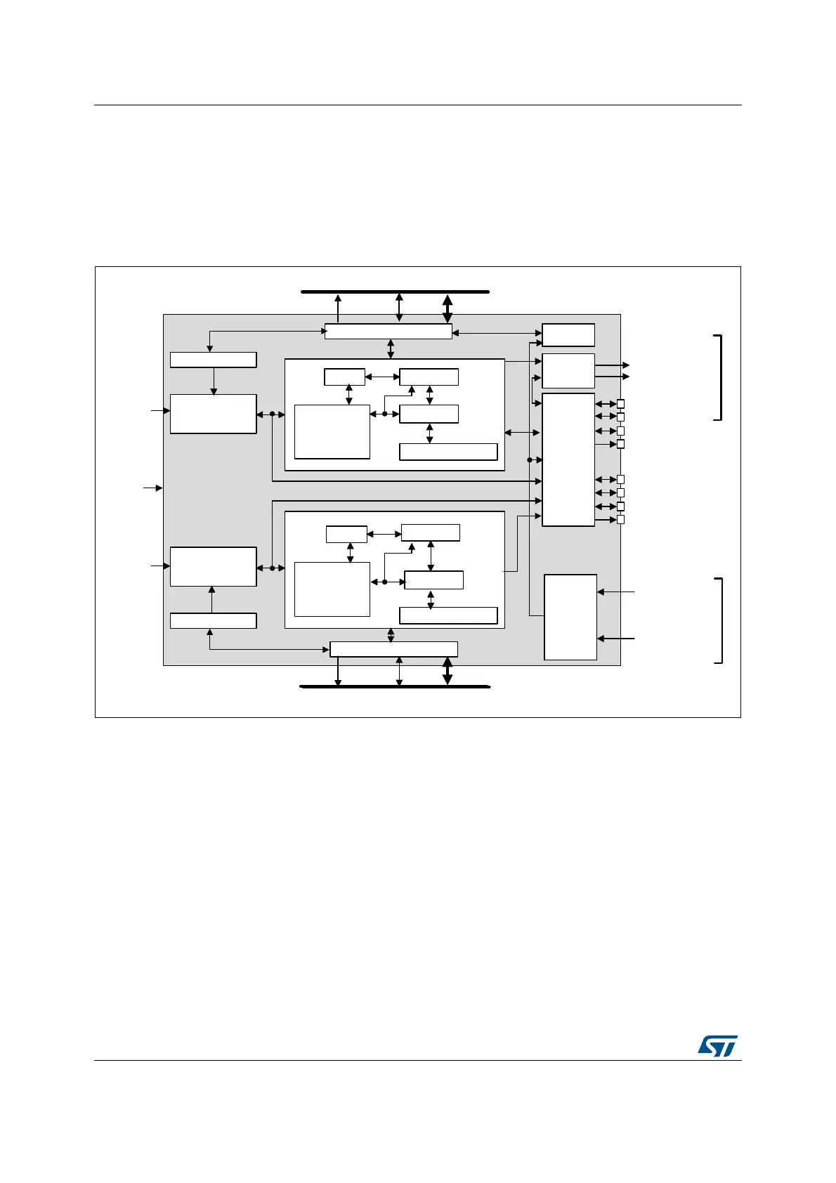
28.3.1 SAI block diagram
Figure 354 shows the SAI block diagram while Table 171 and Table 172 list SAI internal and
external signals.
Figure 354. SAI functional block diagram
The SAI is mainly composed of two audio sub-blocks with their own clock generator. Each
audio block integrates a 32-bit shift register controlled by their own functional state machine.
Data are stored or read from the dedicated FIFO. FIFO may be accessed by the CPU, or by
DMA in order to leave the CPU free during the communication. Each audio block is
independent. They can be synchronous with each other.
An I/O line controller manages a set of 4 dedicated pins (SD, SCK, FS, MCLK) for a given
audio block in the SAI. Some of these pins can be shared if the two sub-blocks are declared
as synchronous to leave some free to be used as general purpose I/Os. The MCLK pin can
be output, or not, depending on the application, the decoder requirement and whether the
audio block is configured as the master.
If one SAI is configured to operate synchronously with another one, even more I/Os can be
freed (except for pins SD_x).
The functional state machine can be configured to address a wide range of audio protocols.
Some registers are present to set-up the desired protocols (audio frame waveform
generator).
06Y9
),)2 ),)2FWUO
&RQILJXUDWLRQ
DQGVWDWXV
UHJLVWHUV
)60
ELWVKLIWUHJLVWHU
$XGLREORFN$
),)2
),)2FWUO
&RQILJXUDWLRQ
DQGVWDWXV
UHJLVWHUV
)60
ELWVKLIWUHJLVWHU
$XGLREORFN%
&ORFNJHQHUDWRU
$XGLREORFN$
6$,B$&5
6$,B%&5
&ORFNJHQHUDWRU
$XGLREORFN%
$3%,QWHUIDFH
$3%,QWHUIDFH
6$,B*&5
6\QFKUR
FWUORXW
,2/LQH0DQDJHPHQW
6$,
)6B$
6'B$
6&.B$
0&/.B$
)6B%
6'B%
6&.B%
0&/.B%
ELW$3%EXV
ELW$3%EXV
VDLBDBJEOBLW
VDLBEBJEOBLW
VDLBEBGPD
VDLBDBGPD
7RRWKHU6$,%ORFNV
VDLBV\QFBRXWBVFN
VDLBV\QFBRXWBIV
VDLBDB
NHUBFN
VDLBEB
NHUBFN
VDLBSFON
6\QFKUR
LQ
)URPRWKHU6$,%ORFNV
VDLBV\QFBLQBVFN
VDLBV\QFBLQBIV