Digital-to-analog converter (DAC) RM0390
402/1328 RM0390 Rev 4
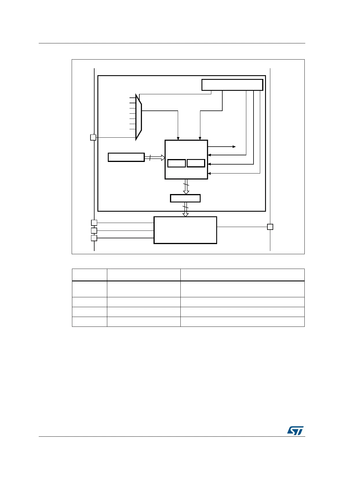
Figure 92. DAC channel block diagram
Note: Once the DAC channelx is enabled, the corresponding GPIO pin (PA4 or PA5) is
automatically connected to the analog converter output (DAC_OUTx). In order to avoid
parasitic consumption, the PA4 or PA5 pin should first be configured to analog (AIN).
14.3 DAC functional description
14.3.1 DAC channel enable
Each DAC channel can be powered on by setting its corresponding ENx bit in the DAC_CR
register. The DAC channel is then enabled after a startup time t
WAKEUP
.
Table 93. DAC pins
Name Signal type Remarks
V
REF+
Input, analog reference
positive
The higher/positive reference voltage for the DAC,
1.8 V V
REF+
V
DDA
V
DDA
Input, analog supply Analog power supply
V
SSA
Input, analog supply ground Ground for analog power supply
DAC_OUTx Analog output signal DAC channelx analog output
9
''$
9
66$
9
5()
'$&B28 7
&RQWUROORJLF[
'+5[
ELW
ELW
/)65[
WULDQJOH[
'0 $UHTXHVW[
76( /[>@ELWV
7,0B7 5*2
7,0B75*2
7,0B7 5*2
7,0B7 5*2
7,0B7 5*2
7,0B75*2
(;7,B
'0$(1[
7(1[
0$03[>@ELWV
:$9(1[>@ELWV
6:75,*[
'25[
'LJLWDOWRDQDORJ
FRQYHUWHU[
ELW
'$&FRQWUROUHJLVWHU
DLG
7ULJJHUVHOHFWRU[
 Loading...


