RM0390 Rev 4 251/1328
RM0390 Flexible memory controller (FMC)
324
The Write FIFO can be disabled by setting the WFDIS bit in the FMC_BCR1 register.
At startup the FMC pins must be configured by the user application. The FMC I/O pins which
are not used by the application can be used for other purposes.
The FMC registers that define the external device type and associated characteristics are
usually set at boot time and do not change until the next reset or power-up. However, the
settings can be changed at any time.
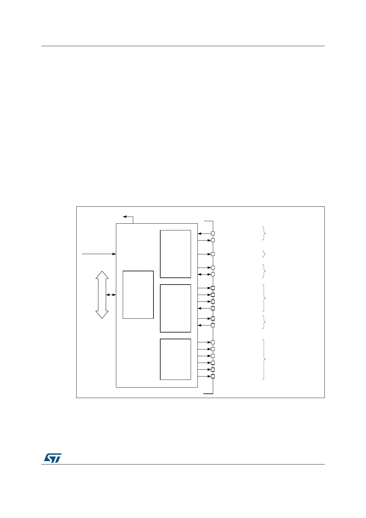
11.2 FMC block diagram
The FMC consists of the following main blocks:
• The AHB interface (including the FMC configuration registers)
• The NOR Flash/PSRAM/SRAM controller
• The SDRAM controller
• The external device interface
The block diagram is shown in the figure below.
Figure 32. FMC block diagram
069
125365$0
VLJQDOV
)0&B1(>@
)0&B1/RU1$'9
)0&B'>@
)0&B12(
)0&B1:(
)0&B1%/>@
)0&B1&(
)0&B,17
)0&B&/.
)0&B6'1:(
)0&B6'&.(>@
)0&B6'1(>@
)0&B15$6
)0&B1&$6
)0&B$>@
)0&B6'&/.
)0&LQWHUUXSWVWR19,&
)URPFORFN
FRQWUROOHU
125365$0
PHPRU\
FRQWUROOHU
&RQILJXUDWLRQ
UHJLVWHUV
1$1'
PHPRU\
FRQWUROOHU
6'5$0
FRQWUROOHU
+&/.
)0&B1:$,7
6'5$0VLJQDOV
1$1'VLJQDOV
125365$065$0
VKDUHGVLJQDOV
6KDUHGVLJQDOV
125365$065$0
VKDUHGVLJQDOV
 Loading...


