RM0390 Rev 4 163/1328
RM0390 Reset and clock control (RCC)
175
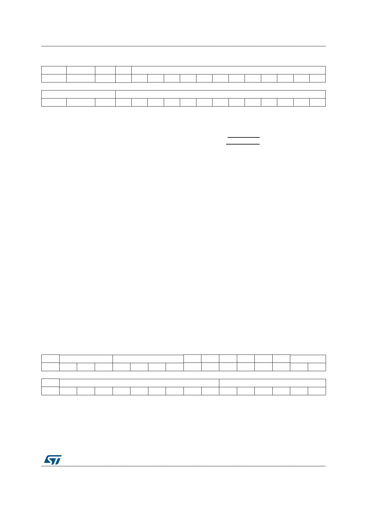
6.3.23 RCC PLLI2S configuration register (RCC_PLLI2SCFGR)
Address offset: 0x84
Reset value: 0x2400 3010
Access: no wait state, word, half-word and byte access.
This register is used to configure the PLLI2S clock outputs according to the formulas:
f
(VCO clock)
= f
(PLLI2S clock input)
× (PLLI2SN / PLLI2SM)
f
(PLL I2S clock output)
= f
(VCO clock)
/ PLLI2SR
f
(PLL SPDIFRX clock output)
= f
(VCO clock)
/ PLLI2SP
31 30 29 28 27 26 25 24 23 22 21 20 19 18 17 16
SSCGEN SPREADSEL Res. Res. INCSTEP
rw rw rw rw rw rw rw rw rw rw rw rw rw
15 14 131211109876543210
INCSTEP MODPER
rw rw rw rw rw rw rw rw rw rw rw rw rw rw rw rw
Bit 31 SSCGEN: Spread spectrum modulation enable
This bit is set and cleared by software.
0: Spread spectrum modulation DISABLE. (To write after clearing CR[24]=PLLON bit)
1: Spread spectrum modulation ENABLE. (To write before setting CR[24]=PLLON bit)
Bit 30 SPREADSEL: Spread Select
This bit is set and cleared by software.
To write before to set CR[24]=PLLON bit.
0: Center spread
1: Down spread
Bits 29:28 Reserved, must be kept at reset value.
Bits 27:13 INCSTEP: Incrementation step
These bits are set and cleared by software. To write before setting CR[24]=PLLON bit.
Configuration input for modulation profile amplitude.
Bits 12:0 MODPER: Modulation period
These bits are set and cleared by software. To write before setting CR[24]=PLLON bit.
Configuration input for modulation profile period.
31 30 29 28 27 26 25 24 23 22 21 20 19 18 17 16
Res. PLLI2SR[2:0] PLLI2SQ[3:0] Res. Res. Res. Res. Res. Res. PLLI2SP[1:0]
rw rw rw rw rw rw rw rw rw
1514131211109876543210
Res. PLLI2SN[8:0] PLLI2SM[5:0]
rw rw rw rw rw rw rw rw rw rw rw rw rw rw rw
 Loading...


