System configuration controller (SYSCFG) RM0390
196/1328 RM0390 Rev 4
)
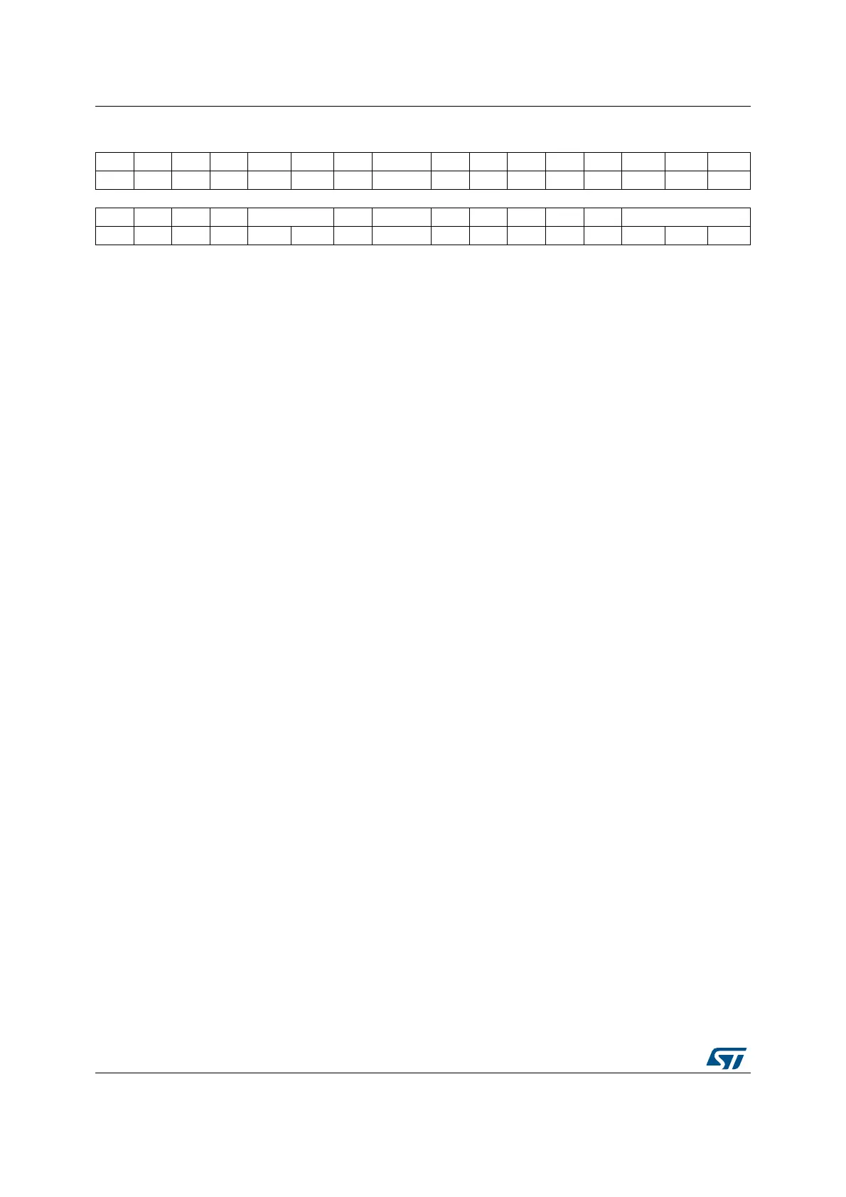
31 30 29 28 27 26 25 24 23 22 21 20 19 18 17 16
Res. Res. Res. Res. Res. Res. Res. Res. Res. Res. Res. Res. Res. Res. Res. Res.
15 14 13 12 11 10 9 8 7 6 5 4 3 2 1 0
Res. Res. Res. Res. SWP_FMC Res. Res. Res. Res. Res. Res. Res. MEM_MODE[2:0]
rw rw rw rw rw
Bits 31:12 Reserved, must be kept at reset value.
Bits 11:10 SWP_FMC: FMC memory mapping swap
Set and cleared by software. These bits are used to swap the FMC SDRAM
Banks 1/2 from address 0xC000 0000 and 0xD000 0000 to address 0x6000
0000 and 0x7000 0000 to enable the code execution from SDRAM Banks
without a physical remapping at 0x0000 0000 address. NOR/PSRAM Bank,
which is by default mapped at 0x6000 0000, is remapped at 0xC000 0000 when
SDRAM bank1 is mapped at 0x6000 0000.
00: No FMC memory mapping swap
01: SDRAM banks mapping are swapped. SDRAM Bank 1 and 2 are mapped at
0x6000 0000 and 0x7000 0000 address, respectively. NOR/PSRAM Bank is
mapped at 0xC000 0000.
10: Reserved
11: Reserved
Bits 9:3 Reserved, must be kept at reset value.
Bits 2:0 MEM_MODE: Memory mapping selection
Set and cleared by software. This bit controls the memory internal mapping at
address 0x0000 0000. After reset these bits take the value selected by the Boot
pins (except for FMC).
000: Main Flash memory mapped at 0x0000 0000
001: System Flash memory mapped at 0x0000 0000
010: FMC Bank1 (NOR/PSRAM 1 and 2) mapped at 0x0000 0000
011: Embedded SRAM (SRAM1) mapped at 0x0000 0000
100: FMC/SDRAM Bank 1 mapped at 0x0000 0000
Other configurations are reserved
Note: Refer to Section 2.2.2: Memory map and register boundary addresses for
details about the memory mapping at address 0x0000 0000.
 Loading...


