RM0390 Rev 4 317/1328
RM0390 Flexible memory controller (FMC)
324
Note: Before modifying the RBURST or RPIPE settings or disabling the SDCLK clock, the user
must first send a PALL command to make sure ongoing operations are complete.
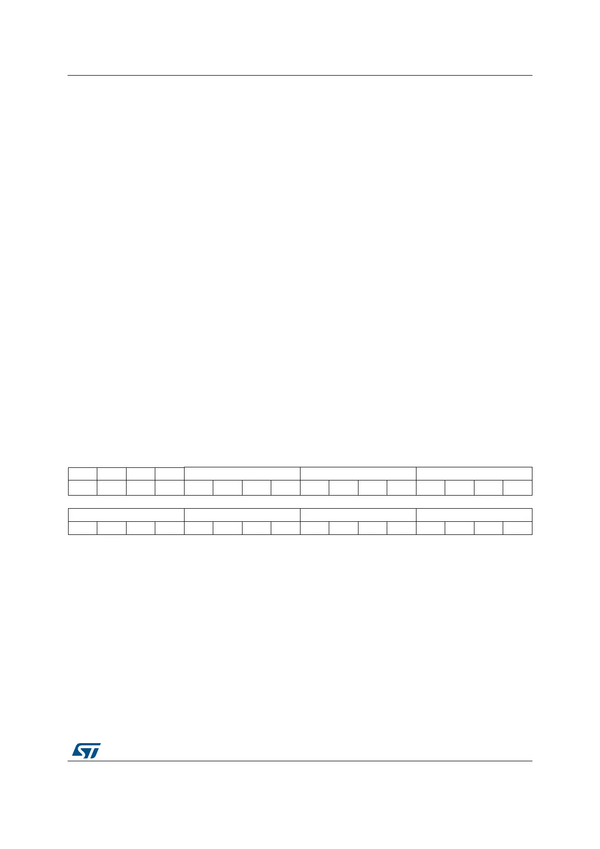
SDRAM Timing registers 1,2 (FMC_SDTR1,2)
Address offset: 0x148 + 4 * (x – 1), x = 1,2
Reset value: 0x0FFF FFFF
This register contains the timing parameters of each SDRAM bank
Bits 5:4 MWID[1:0]: Memory data bus width.
These bits define the memory device width.
00: 8 bits
01: 16 bits
10: reserved
11: reserved.
Bits 3:2 NR[1:0]: Number of row address bits
These bits define the number of bits of a row address.
00: 11 bit
01: 12 bits
10: 13 bits
11: reserved.
Bits 1:0 NC[1:0]: Number of column address bits
These bits define the number of bits of a column address.
00: 8 bits
01: 9 bits
10: 10 bits
11: 11 bits.
31 30 29 28 27 26 25 24 23 22 21 20 19 18 17 16
Res. Res. Res. Res. TRCD TRP TWR
rw rw rw rw rw rw rw rw rw rw rw rw
1514131211109876543210
TRC TRAS TXSR TMRD
rw rw rw rw rw rw rw rw rw rw rw rw rw rw rw rw
Bits 31:28 Reserved, must be kept at reset value
Bits 27:24 TRCD[3:0]: Row to column delay
These bits define the delay between the Activate command and a Read/Write command in number
of memory clock cycles.
0000: 1 cycle.
0001: 2 cycles
....
1111: 16 cycles
 Loading...