Embedded Flash memory (FLASH) RM0453
150/1461 RM0453 Rev 1
write access privilege and can only be written by a privileged access. Unprivileged write
access from is ignored and an illegal access event is generated. Unprivileged read access
is still allowed.
This register, except for C2OPT and SBRV bits, is further write protected by HDPADIS when
HDPAD = 0. Write protected bits can only be written when HDPADIS = 0. When
HDPADIS = 1, write access is ignored. Read access returns register data.
C2OPT and SBRV bits are further protected by C2BOOT_LOCK,. The protected bits can
only be accessed when C2BOOT_LOCK = 0. When C2BOOT_LOCK = 1, write access is
ignored and read access returns register data.
Written values are only taken into account after OBL.
There are no read restrictions.
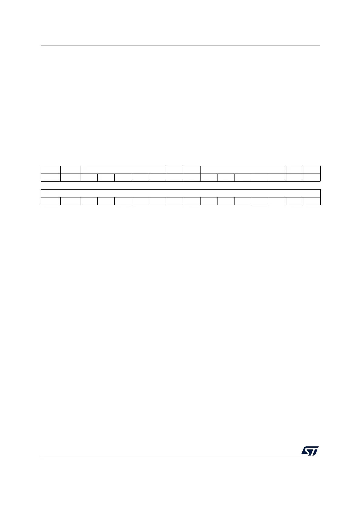
31 30 29 28 27 26 25 24 23 22 21 20 19 18 17 16
C2OPT NBRSD SNBRSA[4:0] Res. BRSD SBRSA[4:0] Res. Res.
rw rw rw rw rw rw rw rw rw rw rw rw rw
1514131211109876543210
SBRV[15:0]
rw rw rw rw rw rw rw rw rw rw rw rw rw rw rw rw
Bit 31 C2OPT: CPU2 boot reset vector memory selection
This bit can only be accessed by software when C2BOOT_LOCK = 0
0: SBRV offset addresses SRAM1 or SRAM2, from start address 0x2000 0000 + SBRV.
Note: SBRV offset value must be kept within the SRAM area.
1: SBRV offset addresses the Flash memory, from start address 0x0800 0000 + SBRV.
Bit 30 NBRSD: “non-backup” SRAM1 security disable
This bit is write protected when HDPAD = 0 and HDPADIS = 1.
When FSD = 1, SRAM1 is non-secure whatever the value of this NBRSD bit.
o (and FSD = 0): SRAM1 is secure. SNBRSA[4:0] contains the start address of the first 1-
Kbyte page of the secure “non-backup” SRAM1 area.
1 (and FSD = 0): SRAM1 is non-secure.
Bits 29:25 SNBRSA[4:0]: secure “non-backup” SRAM1 start address
This bit is write protected when HDPAD = 0 and HDPADIS = 1.
When FSD = NBRSD = 0, SRAM1 is secure. SNBRSA[4:0] contains the start address of
the first 1-Kbyte page of the secure “non-backup” SRAM1 area.
0x00: “non-backup” SRAM1 start address offset 0x0000 0000
0x01: “non-backup” SRAM1 start address offset 0x0000 0400
...
0x1F: “non-backup” SRAM1 start address offset 0x0000 7C00
Bit 24 Reserved, must be kept at reset value.
Bit 23 BRSD: “backup” SRAM2 security disable
This bit is write protected when HDPAD = 0 and HDPADIS = 1.
When FSD = 1, SRAM2 is non-secure whatever the value of this BRSD bit.
0 (and FSD = 0): SRAM2 is secure. SBRSA[4:0] contains the start address of the first 1-
Kbyte page of the secure “backup” SRAM2 area.
1 (and FSD = 0): SRAM2 is non-secure.

 Loading...


