CMS32L051 User Manual |Chapter 5 Universal Timer Unit (Timer4)
www.mcu.com.cn 127 / 703
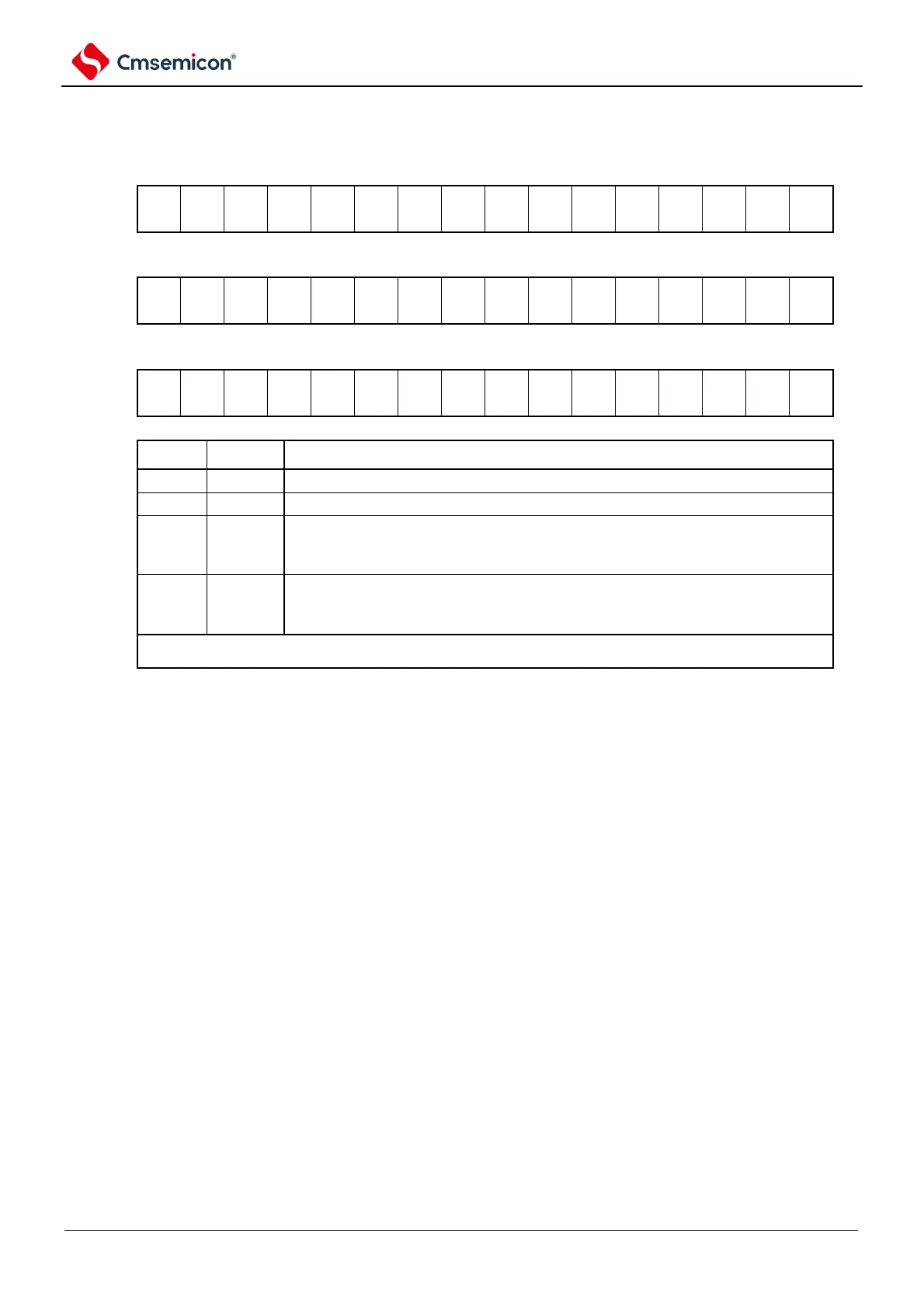
Figure 5-11 Table of timer mode register mns (TMRmn) (3/4)
Symbol
15 14 13 12 11 10 9 8 7 6 5 4 3 2 1 0
TMRmn
(n=2)
Symbol
15 14 13 12 11 10 9 8 7 6 5 4 3 2 1 0
TMRmn
(n=1, 3)
Symbol
15 14 13 12 11 10 9 8 7 6 5 4 3 2 1 0
TMRmn
(n=0)
Valid edge selection for the TImn pin
Bilateral edges (when measuring low widths)
Start trigger: falling edge,
snap trigger: rising edge
Bilateral edges (when measuring high widths)
Start trigger: rising edge,
snap trigger: falling edge
When the STSmn2~STSmn0 bits are not 010B and are specified using a bilateral edge, the CISmn1~CISmn0
positions must be 10B.
Note 1: bit11 is a read-only bit, fixed to 0, ignoring write operations.
Remark: m: unit number (m=0,1) n: channel number (n=0~3).