CMS32L051 User Manual |Chapter 5 Universal Timer Unit (Timer4)
www.mcu.com.cn 203 / 703
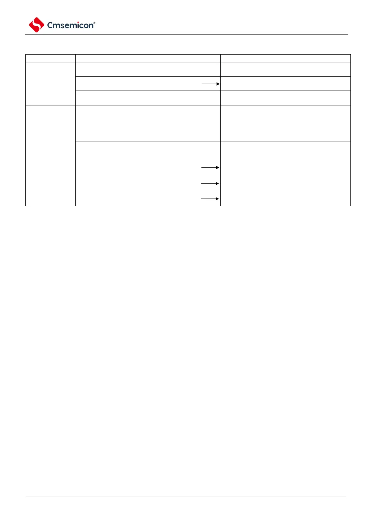
Figure 5-77 Operation procedure for multiple PWM output function (in case of 2 PWM outputs) (1/2)
software operation hardware state
Timer Unit m input clock is in stopped state (stop
providing clock, not able to write into registers)
set TM4mEN bit of peripheral enable register 0 (PER0) to '1'
Timer Unit m input clock is in active state, all channels
in operation stopped state.
configure Timer clock selection register m(TPSm), confirm
CKm0~CKm3 clock frequency
configure using timer mode register mn,mp (TMRmn,TMRmp) of
2 channels (confirm channel operation mode).
Configure interal(period) value of Timer data register mn
(TDRmn) of master control channel, and configure duty-cycle of
slave channel TDRmp.
channel in operation stopped state (providing clock,
consume portion of power)
slave channel configuration
set TOMmp bit and TOLmq bit of timer output mode register
m(TOMm) to '1' (slave channel output mode).
Configure TOLmp and Tomq bit to '0'.
Configure TOmp bit and Tomq bit, confirm TOmp and Tomq
otuput initial voltage.
Set TOEmp bit and TOEmq to '1', enable TOmp and Tomq
output.
Set port regsiter and port mode regsiter to '0'.
T0mp pin in Hi-Z output state.
When port mode register set to output mode and port
register as '0', output T0mp and T0mq initial configured
voltage level.
Because channel is in operation stopped state, thus
T0mp and T0mq remains unchange. T0mp pin and T0mq
pin output T0mp and T0mq configured voltage level.
Timer 4 initial
configuration
Channel Initial
configuration