CMS32L051 User Manual |Chapter 12 Universal Serial Communication Unit
www.mcu.com.cn 375 / 703
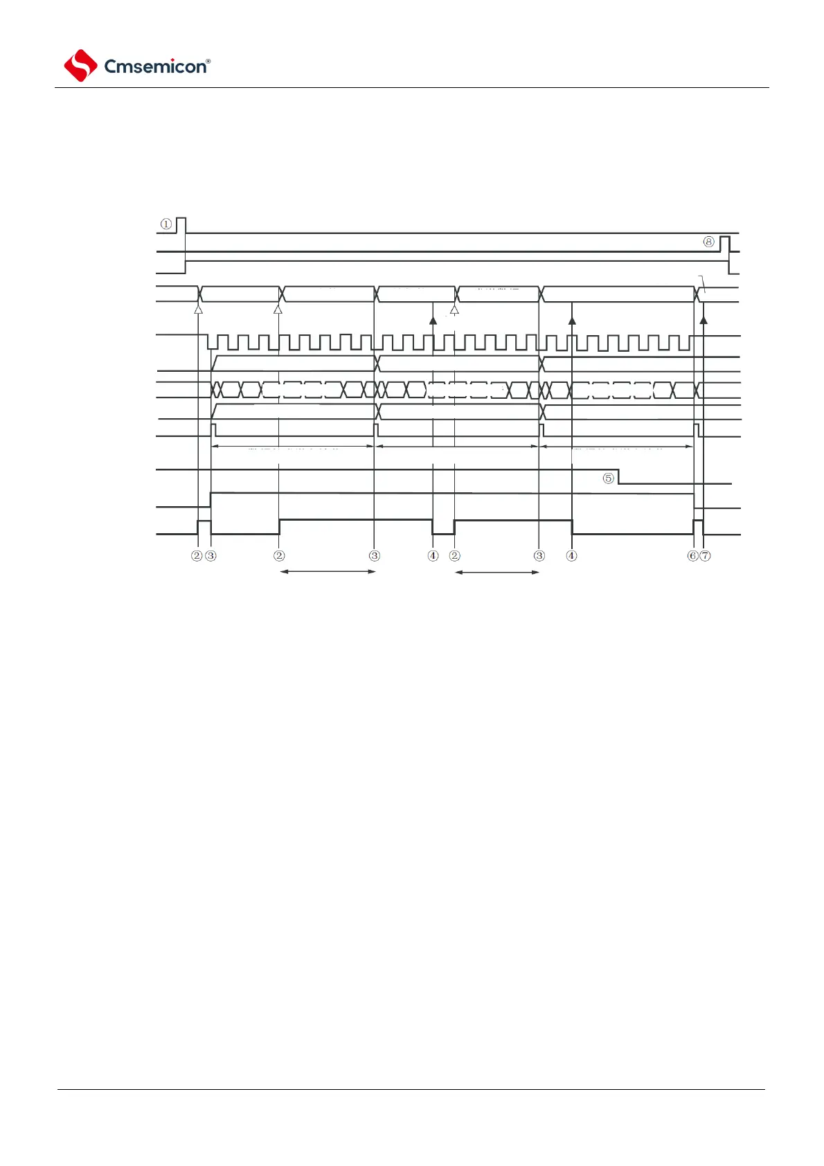
(4) Process flow (continuous send and receive mode).
Figure 12-67 Timing diagram of slave transmit and receive (continuous transmit and receive mode)
(type 1: DAPmn=0, CKPmn=0).
SCLKp pin
INTSSPIp
shift register mn
TSFmn
SDRmn
SEmn
STmn
SSmn
BFFmn
MDmn0
SDOP pin
SDIp pin
transmit data1
transmit data 2
transmit data 3data reception 1
data reception 2
data reception 3
data reception 1 data reception 2
data reception 3
transmit data1
transmit data 2
transmit data 3
Receiving&shift operation Receiving&shift operation Receiving&shift operation
data transmission and reception data transmission and reception data transmission and reception
Read
Write
Read Read
WriteWrite
Note1
Note2 Note2
Note 1 If the BFFmn bit of the serial status register mn (SSRmn) is 1 (valid data is saved in the serial data register mn
(SDRmn ) to write the send data to the SDRmn memory, and override the sent data.
2. If the SDRmn register is read during this period, the transmitted data can be read. At this point, the transfer run is not
affected.
Notice The MDmn0 bit of the serial mode register mn (SMRmn) can be overridden even during operation. However, in
order to catch up with the end of the transmission interruption of the last transmitted data, it must be overwritten
before the last bit of transmission begins.
Remark 1. (1) to (8) in the figure corresponds to (1) to (8) in Figure 12-68 of Slave Send and Receive (Continuous Send
and Receive Mode).
2.m: Unit number (m=0, 1) n: Channel number (n=0~3) p: SSPI number (p=00, 01, 10, 11, 20, 21)
mn=00~03, 10~11