CMS32L051 User Manual |Chapter 4 Clock Generation Circuit
www.mcu.com.cn 82 / 703
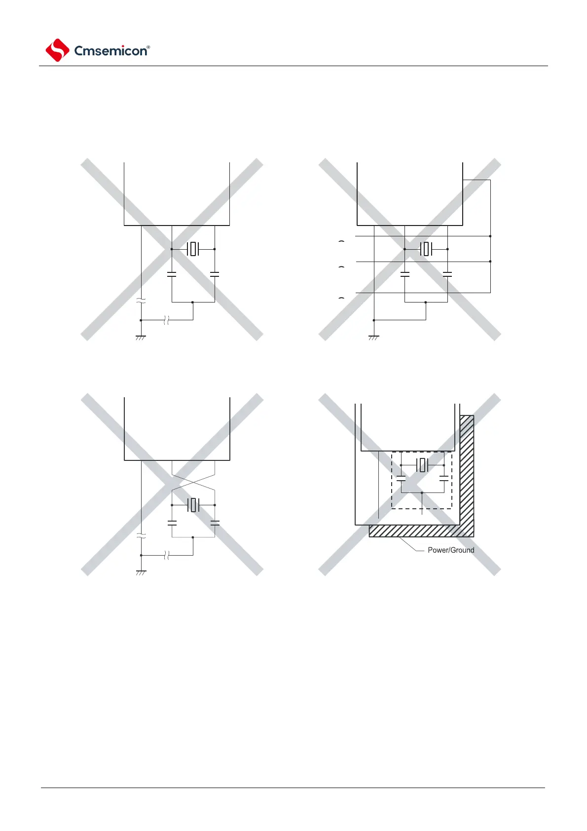
An example of an incorrect resonator connection is shown in Figure 4-15.
Figure 4-15 Example of an incorrect resonator connection (1/2).
(a) The routing connecting the circuit is too long (b) the signal lines cross
(c) X1 and X2 signal line cross-routing (d) X1 and X2 have a power or ground pattern below the
routing
In multilayer boards or bi-panels, power or ground graphics cannot be configured below the routing area of the X1
pin, X2 pin, and resonator (dotted in the figure). The routing cannot produce a capacitive component that affects
the oscillation characteristics.
Note In the case of a subsystem clock, replace X1 and X2 with XT1 and XT2 respectively when reading, and insert a
serial resistor on the XT2 side.