RM0453 Rev 1 1375/1461
RM0453 Debug support (DBG)
1448
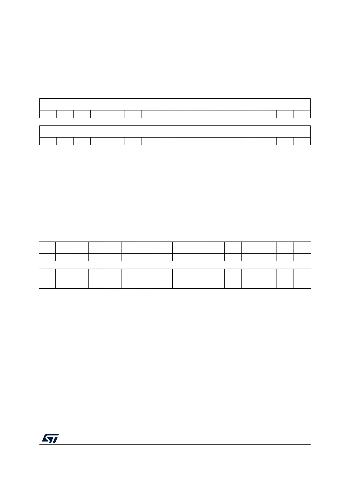
CTI lock access register (CTI_LAR)
Address offset: 0xFB0
Reset value: 0x0000 0000
CTI lock status register (CTI_LSR)
Address offset: 0xFB4
Reset value: 0x0000 0003
31 30 29 28 27 26 25 24 23 22 21 20 19 18 17 16
ACCESS_W[31:16]
rrrrrrrrrrrrrrrr
1514131211109876543210
ACCESS_W[15:0]
rrrrrrrrrrrrrrrr
Bits 31:0 ACCESS_W[31:0]: write access enable
Enables write access to some CTI registers by processor cores (debuggers do not need to
unlock the component).
0xC5AC CE55: Write access enabled
Other values: Write access disabled
31 30 29 28 27 26 25 24 23 22 21 20 19 18 17 16
Res. Res. Res. Res. Res. Res. Res. Res. Res. Res. Res. Res. Res. Res. Res. Res.
1514131211109876543210
Res. Res. Res. Res. Res. Res. Res. Res. Res. Res. Res. Res. Res.
LOCK
TYPE
LOCK
GRANT
LOCK
EXIST
rrr
Bits 31:3 Reserved, must be kept at reset value.
Bit 2 LOCKTYPE: size of the CTI_LAR register
0: 32 bits
Bit 1 LOCKGRANT: current status of lock.
This bit is always read as zero by an external debugger.
0: Write access permitted
1: Write access blocked (only reads allowed)
Bit 0 LOCKEXIST: lock control mechanism availability
This bit is always read as zero by an external debugger.
0: No lock control mechanism
1: Lock control mechanism implemented
 Loading...


